Ion Beam Sputtering is a deposition technique that uses an ion source to sputter a target material onto a substrate. The system includes a rotary multitarget assembly, a substrate, and an ion source used to sputter the target and deposit it onto the substrate surface. Using gas (Ar) injection into the ion gun, a high electric field causes gas ionization, creating a plasma inside the source region. The ions generated in the plasma are accelerated from the source to the target, creating a collimated ion beam with a well-defined ionic energy and density. This beam impacts the target material, causing it to sputter towards the substrate. Plasma in IBS is confined within the ion source, allowing the chamber pressure to be maintained low. An additional ion beam source can be used to bombard the substrate with Ar ions to improve the density or reactive gas ions to maintain stoichiometry. Substrate heating during deposition can improve overall sputtering performance. Ion Beam Sputtering: the optimal choice for dense, smooth and uniform coatings Ion beam applications encompass a wide range of processes that range over deposition, etching, or their combination. These applications include laser facet coating, mirrors for ring laser gyroscopes, X-ray optics, infrared sensors, telecom optic filters, Magnetic Random Access Memory (MRAM), dielectrics, spintronics, and superconductors. KEY FEATURES - Low pressure processing (10-5 to 10-4 Torr range) - Reduced porosity (higher density) in deposited films (low pressure means reduced included gas) - High quality optical films with smooth surfaces - Single Ion Beam or Dual Ion Beam configuration sources can be combined for DC, DC pulsed, RF depending on target material and layers that will be deposited - Substrate conditioning from –35 °C up to 800 °C - Reactive gases (O2, N2, H2, etc.) can be added for direct reaction during deposition process - Optional automatic or manual load lock with optional pre-heating and/or plasma treatments - Optional full optical thickness monitor for an unlimited number of layers by T% or R% wavelength scans on the coated substrates APPLICATIONS - Consumer Electronics - Automotive Industry - Aerospace and Defence - Healthcare and medical devices - Optics and Photonics - Energy storage TECHNICAL DATA Base pressure HV < 1x10⁻⁶ mbar Base pressure UHV < 1x10⁻⁹ mbar Pumping System Turbomolecular, Cryo, TSP or combined Cryo / Turbo for ultimate vacuum and processes Ion Sources Single or Dual (gridded or not gridded) DC, DC pulsed, RF Source Power Evaporation, Electron Beam, Magnetron sputtering Chamber Size Up to 12” Deposition area Rotation: up to 50 rpm, optional planetary configuration; Tilt: ±45°; Offset (Z or X): up to 100 mm Substrate rotation Up to 800 °C Substrate tilt One or more reactive gases (O2, H2, N2, etc.) Reactive process Up to 1% Source combination Programmable quartz crystal thickness controller and/or in situ optical monitor Process control Manual in main Chamber or by Load Lock with manual or automatic manipulator Substrate load Single or Multiple Load Locks, can be motorized with multiple substrate holder Load lock Optional multi wafer charge system up to 25 wafers Deposited materials Metals, Oxides, Nitrides, Carbides, Semiconductors, Carbon Based Materials
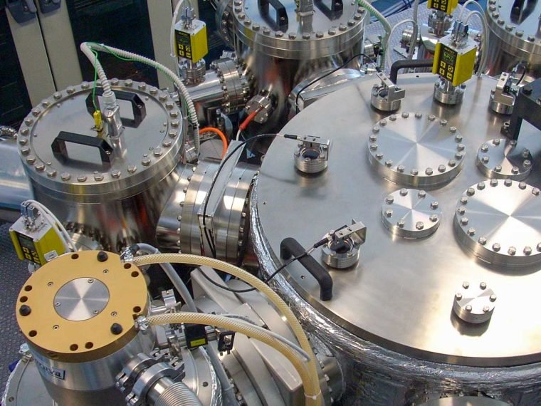
We design and manufacture complete deposition thin film processing equipment solutions for R&D or pilot production applications. Based on most advanced technologies, our products include a complete array of turnkey systems using chemical or physical deposition, sputtering or etchnig processes
CATEGORY
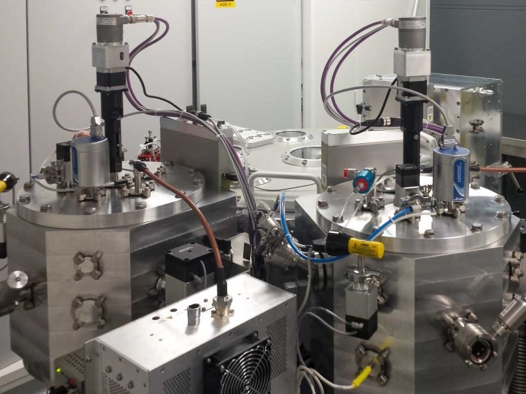
In order to satisfy the need to obtain products through deposition with different technologies, we are able to design and build multi-process machines able to operate automatically both in sequential and single mode
CATEGORY
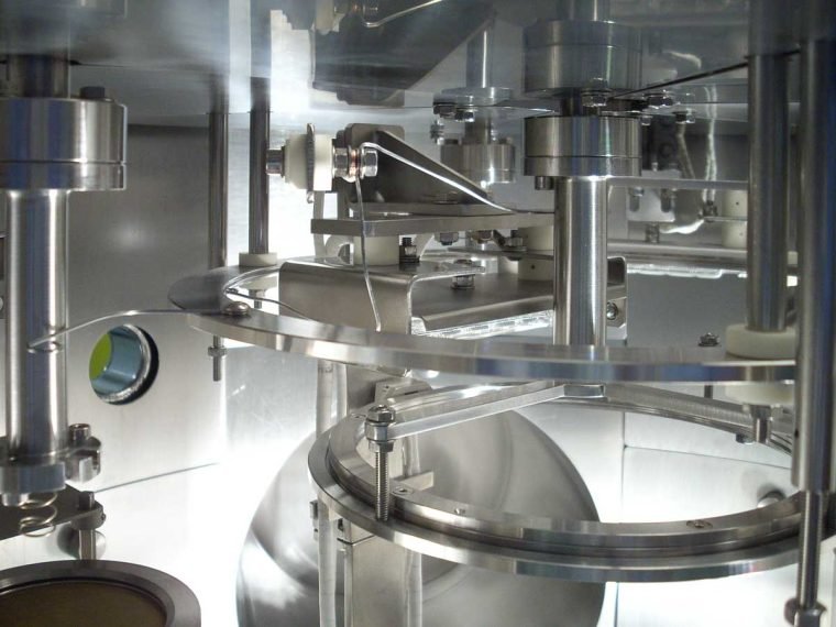
We pay special attention to specific customer needs, offering complete tailor made systems designed to achieve the performance required by the customer and provided with a process guarantee
CATEGORY
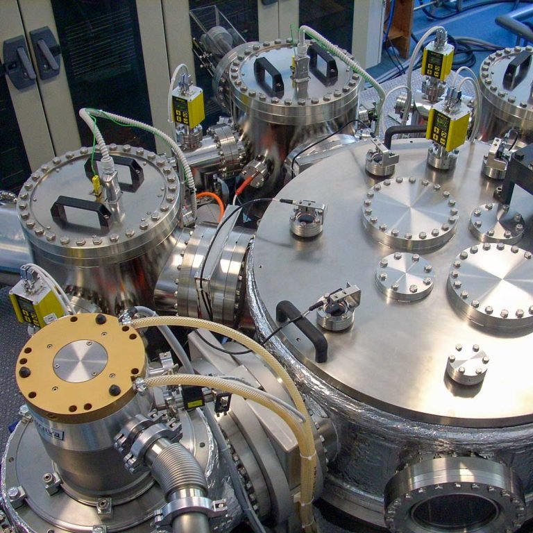
Plasma-enhanced chemical vapor deposition is a plasma-based deposition method used to deposit material on a substrate surface. PECVD is commonly used for depositing silicon oxide/nitride, hydrogenated amorphous and microcrystalline silicon and carbon, Diamond-like carbon (DLC), semiconductors and oxides. The process involves introducing a gas mixture into the vacuum chamber, where a plasma is generated. The process gases are ionized and decomposed into ions and radicals, which react with the substrate via chemical reactions, leading to the deposition of a thin film on the substrate. The plasma can be generated using different methods such as radio frequency (RF), alternating current (AC), or direct current (DC) discharge between two electrodes. PECVD offers a higher deposition rate while maintaining a lower temperature compared to thermal CVD Applications PECVD is used to produce high-quality semiconductor and dielectric films required for various applications, like low and high-power semiconductor devices, photovoltaic solar cells' active layers, metal-insulator-metal (MIM) capacitors, laser diodes, sensors, detectors, LEDs, thin film transistors, and more. - Consumer Electronics - Automotive Industry - Solar energy - Aerospace and Defence - Healthcare and medical devices - Optics and Photonics - Wear resistant coatings Key features - RF showerhead electrode for uniform electric field and gas distribution - Modular process gas manifold with mass flow controllers for up to 12 gases - Optional vapor source controller for liquid Precursor (i.e. TEOS) with tank/cylinder in a closed cabinet for safe refill - Automatic process pressure control - Alternatively Hot Wire CVD - In situ spectroscopic plasma monitoring - Optional automatic or manual load lock (optional pre-heating and/ or plasma treatments) - Optional wide range optical thickness monitor for the control of layer thickness - Optional in situ spectroscopic ellipsometry for thickness measurement Deposited materials Metals, Oxides, Nitrides, Carbides, Semiconductors, Carbon Based Materials, Organics Plasma Enhanced CVD - the right choice for obtaining large area compound materials mixing gaseous and/or liquid precursors at any temperature
CATEGORY
