By Vmicro
Celgard® 2500 AFM Sample - Ready-to-use Celgard® 2500 film sample. - Mounted and packaged in a cleanroom. Sample overview AFM Sample: This AFM demonstration sample was prepared by mounting Celgard® 2500—a 25 µm thick monolayer microporous polypropylene membrane—onto a 12 mm steel disc using an adhesive. The sample itself measures approximately 5 × 5 mm, providing an effective platform to showcase high-resolution AFM topography images. Primary Applications of Celgard® film: High Power Lithium Battery Systems; especially performance-critical applications. Celgard® 2500 Datasheet Celgard is a registered trademark of Celgard LLC. The Celgard name and logo are used exclusively to identify products manufactured by Celgard LLC, and all rights to the trademark are reserved by the company.
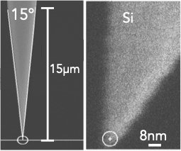
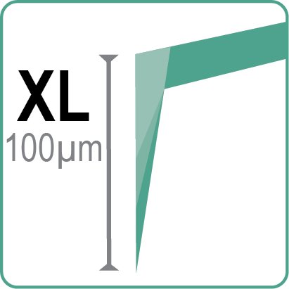
Features - New MEMS technology unlocking probe engineering - Long tip with profiled shape - small cone angle - TrueTipView: Precise tip visibility thus accurate landing on sample - Vertical sidewalls probe chip for easy handling Applications - Topography imaging in oscillating modes - Tapping mode - Non-contact mode - True non-contact TM - Roughness measurements - Nanoscale imaging on highly corrugated samples - Challenging aspect ratios Specifications Specifications Tilted tip design: Compensates for the AFM head mounting angle, ensuring accurate data on diverse sample surfaces. Tip height 30 µm: Enables imaging of deeper or difficult-to-access sample regions. Half-cone angle <10°: Minimizes tip-sample convolution, ensuring more accurate morphological measurements. Guaranteed tip radius <10 nm: Provides reliable resolution for advanced AFM applications.
CATEGORY
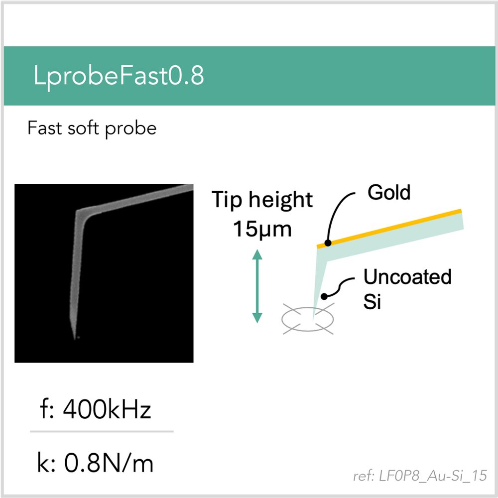
LF0P8Au-Si15 | Lprobe fast AFM probe | Vmicro Features - New MEMS technology - Highly profiled tip with angle engineering - Tip visibility provides accurate landing - Vertical sidewall chip for safe handling Applications - Imaging of cells, bacteria, and tissues in liquid or air - Fast peakForce Tapping TM mode - Fast Wavemode TM mode - High-resolution imaging of polymers and composite materials Specifications - Frequency: 400.0 kHz (nominal), 200-600 range - Spring constant: 0.8 N/m (nominal), 0.2-3 range - Tip height H t: 15.0 µm (nominal), 05-60 range - Tip apex radius: 7.0 nm (nominal), 2-10 range - Tip side angle θ: 22.0 ° (nominal), +/-0.5° - Tip-cantilever angle α: 112.0 ° (nominal), +/-0.5° - Cantilever length L c: 40.0 µm (nominal), +/-1 - Cantilever width W c: 10.0 µm (nominal), +/-1 - Cantilever thickness T c: 0.65 µm (nominal), +/-0.15 - Cantilever backside coating: Au - Tip-side coating: Uncoated - Tip and cantilever material: p-doped Silicon 0.01-0.02 ohm-cm - Chip dimensions: 3.4x1.6x0.4 mm Cantilever & tip details
CATEGORY
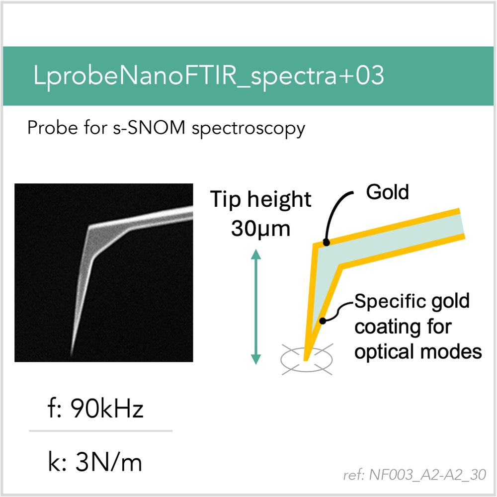
NF003A2-A230 | Lprobe nano-FTIR AFM probe | Vmicro Features - PDMS-free and contamination-controlled - New MEMS technology - Long tip increases spectral range - Highly profiled tip with angle engineering - Precise tip visibility enables accurate landing on sample - Vertical sidewall chip for safe handling Applications - Enhanced s-SNOM spectroscopy in the mid-infrared region - s-SNOM imaging in the mid-infrared region - Soft probe, optimal for combined s-SNOM and KPFM imaging Specifications Frequency: 90.0 kHz nominal, range 50-150 Spring constant: 3.0 N/m nominal, range 1-8 Tip height H t: 30.0 µm nominal, range 15-50 Tip apex radius: 70.0 nm nominal, range 55-90 Tip side angle θ: 15.0° nominal, +/-0.5° Tip-cantilever angle α: 118.0° nominal, +/-0.5° Cantilever length L c: 115.0 µm nominal, +/-1 Cantilever width W c: 40.0 µm nominal, +/-1 Cantilever thickness T c: 1.4 µm nominal, +/-0.15 Cantilever backside coating: A2 Tip-side coating: A2 Tip and cantilever material: p-doped Silicon 0.01-0.02 ohm-cm Chip dimensions: 3.4x1.6x0.4 mm
CATEGORY