By ASML
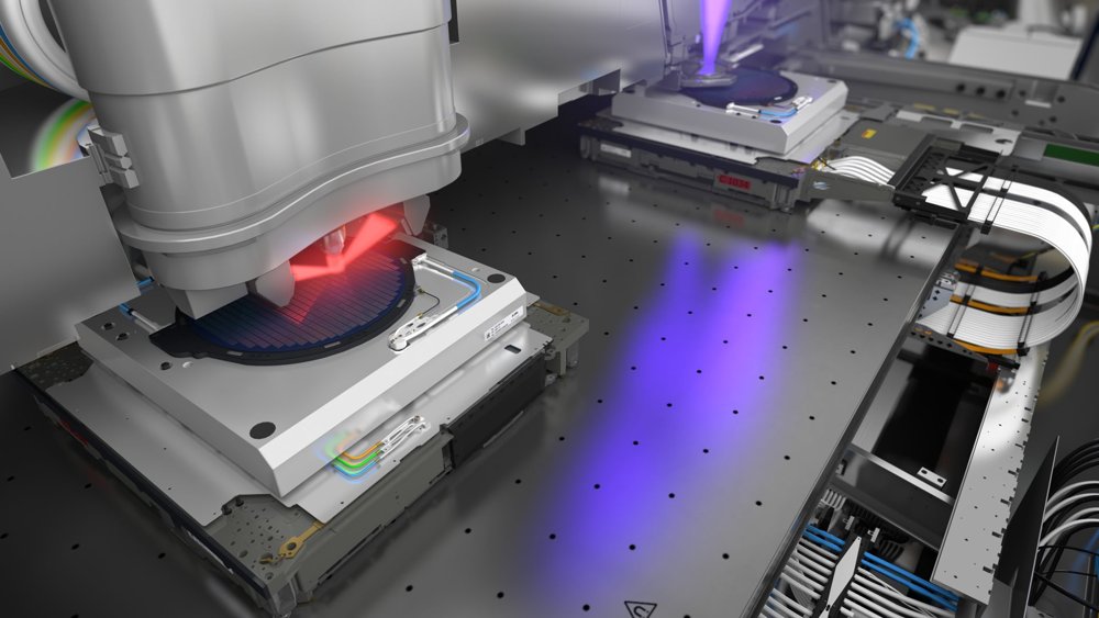
The PAS 5500/450F is the latest and most advanced addition to the i-line Step-and-Scan family. This mass production tool is the successor of the PAS 5500/400 for non-critical applications. This tool has been extended to critical i-line down to 220 nm. The PAS 5500/450F combines the imaging power of a variable 0.48-0.65-NA Carl Zeiss Starlith 4X reduction lens with a high speed scanning stage to deliver a high productivity tool with a superior value of ownership for maximum yield. The system is fully configurable to meet production requirements and offers both ease-of-manufacturing and cost-effectiveness in a high-volume production environment. The PAS 5500/450F continues to raise the bar for imaging performance and productivity in the 200-mm litho market. Technical Specifications High performance configuration Lens including High Performance Imaging Pack Wavelength: 365 nm NA: 0.48–0.65 Resolution: ≤ 220 nm Field size, for reticle with pellicle • Max X: 26.0 mm • Max Y: 33.0 mm CD Uniformity @ 220 nm L/S • BF: ≤ 22 nm • At ± 0.3-μm defocus (@ max NA): ≤ 35 nm CD Uniformity @ 220 nm isolated lines • BF: ≤ 20 nm • At ± 0.2-μm defocus (@ max NA): ≤ 35 nm Distortion (Dynamic): ≤ 20 nm Image Plane Deviation: ≤ 225 nm Astigmatism: ≤ 135 nm Production Throughput including PEP 450F Throughput under ATP conditions 200-mJ/cm 2 exposure dose 16 x 32-mm representative field size • 200-mm wafers, 46 shots: ≥ 150 wph AERIAL Illumination including High Performance Imaging Package Conventional • Intensity: > 5500 mW/cm 2 • σ max: 0.85 • σ min: 0.38 • Integrated slit uniformity: ≤ 1.2% Annular • σ out: 0.38–0.88 • σ in: 0.16–0.64 • Integrated slit uniformity: ≤ 1.2% The ASML refurbished system is configured for high performance. Key Features and Benefits Cost-Effective i-Line High Throughput Scanner, Throughput 150 Wafers per Hour High throughput resulting in superior cost of ownership. Applications The world’s most successful i-line scanner system used in a wide range of processes from critical to non-critical i-line layers ensuring ease-of-manufacturing and cost effectiveness for layers with feature sizes down to 220 nm. High Speed Scanning Stages The latest successful ASML technology with high speed stage innovations are included resulting in the world’s highest 200-mm productivity i-line tools. PAS 5500 Mature Step-and-Scan Body The PAS 5500/450F is based upon the industry-leading 200-mm PAS 5500 Step-and-Scan body. Commonality with PAS 5500 DUV and 193-nm Step-and-Scan Tools for Economic Fab Extensions • Optimized for mix-and-matching • Modular design allowing future improvements to be integrated in the body
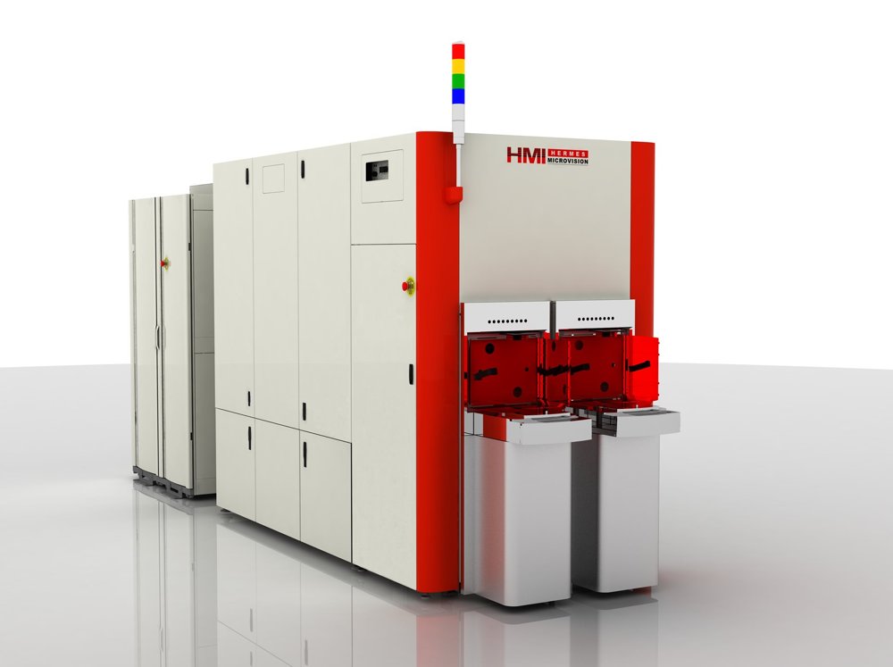
For today’s advanced microchips, defects as small as a couple of nanometers can render the entire chip useless. With its 1-nanometer resolution, e-beam inspection offers just the right kind of eyes to spot those tiny misprints. ASML is at the forefront of developments in e-beam metrology and inspection. E-beam achieves a higher resolution than YieldStar, but it measures more slowly, which means that it’s typically used after the pattern is etched onto the wafer. ‘E’ is for ‘electron’ E-beam technology has been around for decades. The basic concept is that a metal wire is heated until it gives off electrons, which are accelerated and formed into a beam by electric and magnetic fields. Unlike visible and ultraviolet light (but just like extreme ultraviolet light) electron beams must travel in a vacuum so they are not deflected or absorbed before reaching the target. In metrology and inspection in the semiconductor industry, the e-beam scans across the wafer. The electrons strike the surface and penetrate a small distance into the material, generating new 'secondary electrons' before being scattered. Just as with diffraction-based measurements, measuring the scattering of secondary electrons allows us to build up a very high-resolution picture of the surface. The more focused the beam, the smaller the details that can be measured. Speeding up e-beam imaging The tricky thing with e-beam measurements is that they’re quite slow. As a result, they have only typically been used in the early R&D phase of chip manufacturing, where time is less of an issue. ASML is leading the way in speeding up e-beam measurements so that manufacturers can enjoy their benefits in volume production. One way we do that is by developing solutions that focus e-beam measurements on specific hotspots where defects are more likely or more critical. In-line wafer and reticle inspection By speeding up the process and narrowing down the search to specific areas, e-beam can be used directly in the production line for wafer inspection while maintaining productivity levels.
CATEGORY
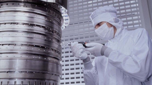
By autumn 2003, the immersion team was able to demonstrate concrete imaging results on the ASML prototype system dubbed the TWINSCAN AT:1150i. "The proto results changed the lithography roadmap almost instantly," Jan says. "We defined a series of new lithography systems in a very short period of time that would directly address the chip industry's resolution struggle."
CATEGORY
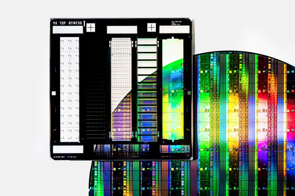
Using the vast amounts of data generated by our systems, computational lithography simulates the manufacturing process with powerful algorithms. These simulations help to design a chip blueprint (the reticle) that contains the pattern to be printed on the wafer. That's how we make sure that our lithography machines print what they should. This technique is called optical proximity correction (OPC) and is often combined with specific illumination optimizations in the lithography system. ASML's industry-leading computational lithography products enable accurate lithography simulations that help to improve chip yield and quality.
CATEGORY