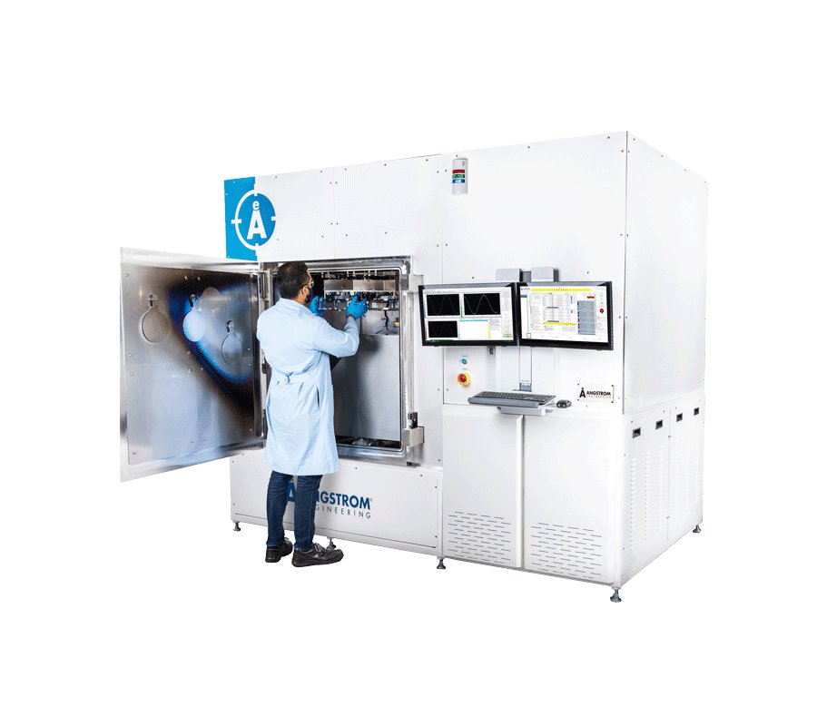
Our Reticle®ion beam sputter deposition systems are designed and engineered to create precise optical films of the highest purity, density, and stability. Angstrom Engineering’s Reticle®systems provide a turn-key solution for those looking to realize any optical design into a high-performance film. When precision is paramount — RETICLE® delivers. This is an ideal system for applications such as antireflective (AR) coatings, highly reflective (HR) coatings, coatings for laser diode bars, telecom optical filters, and vanadium oxide deposition. Angstrom Engineering® designs and engineers each Reticle® platform to provide our partners in the optics community the ability to create the films they need with excellent purity, density, and uniformity, all in a highly repeatable and automated fashion. Reticle® employs Ion Beam Sputter Deposition (IBSD), in which a focused beam of highly energetic ions is accelerated toward a target comprising the material to be deposited. Thoughtful design of the ion beam focusing optics confines the beam entirely to the area of the target, eliminating any risk of contamination. - The IBSD process creates a highly energetic flux of deposition material, leading to films with improved density, hardness, and surface roughness compared to those deposited by evaporation processes. - IBSD takes place in a high vacuum environment, minimizing noble gas inclusion in the deposited film and improving the environmental stability of the coating. - IBSD processes can also employ a secondary ion source for substrate cleaning and energetic assist, substrate heating for reactive deposition, and in-situ optical monitoring or ellipsometry for critical layer thickness termination. Film Quality - All standard Reticle® platforms include an additional gridless end-Hall ion source with hollow cathode neutralizer. - The end-Hall source is optimized for substrate cleaning/etching, ion-assisted deposition, or reactive IBSD processes. - For processes that require deep substrate etching, a selection of gridded DC or RF-ICP ion sources is also available. - The deposition ion source is directed toward a material target which has been optimized in both size and position for the required deposition geometry. - Targets are water-cooled for improved process stability and continuously rotate to prevent beam texturing. For multi-layer depositions, the carousel can be automatically indexed between targets, with up to 8 positions available. - Target rotation and carousel indexing each have torque sense, preventing any process problems due to slips or jams in rotation. - Reticle®can be configured for both high and ultra-high vacuum environments. - High-speed, magnetically levitated turbomolecular pumps serve as the primary high vacuum pump. - An optional cryogenic pump improves base pressure and pumping speed and can be isolated from the chamber during reactive processes with oxygen. - Low-profile chamber bake-out heaters remove moisture from the chamber walls and shielding, improving base pressure and overall process stability. Reticle® employs a selection of gridded RF-ICP ion sources for high-energy deposition. - Available sources include 4, 10, 14, and 22 cm grid configurations with ion energies up to 1200 eV and beam currents greater than 1000 mA. - Self-aligned ion optics are configured specifically for the desired deposition requirements and geometry of your process. - A low-frequency neutralizer ensures stable beam operation without contamination from a traditional filament. - Operation of the RF-ICP source is handled by Aeres®, combining the power of full process flexibility with the ease of one-touch, automated recipe control. Film Uniformity Along with sample rotation, the variable angle stage that is utilized for Reticle® provides for in-built angular motion through the deposition flux. Sweeping the tilt angle can improve film thickness uniformity and sidewall coverage while also avoiding high energy-reflected neutral species for critical processes. Each axis of motion is controlled through Aeres®using precision servo motors, providing better than 0.1 degrees of positional accuracy. Front side infrared heating bulbs tilt with the stage to provide a consistent temperature profile for reactive processes. Planetary rotation integrates a third axis of motion to the variable angle stage. The size, position, and gear ratio of each planet are optimized to provide the absolute best possible film thickness uniformity. Dynamic uniformity shaping is achieved using a flux correction shield between the deposition source and the substrate. The shape of each correction shield can be modelled and empirically optimized for any process. Each correction shield can be tilted in situ to find the perfect balance between film uniformity and deposition rate. Precise Thickness Control In-situ optical monitoring and control is available through Angstrom’s optical monitoring & control package. In-situ ellipsometry provides critical information on the performance of an optical film while it is being deposited. Layer termination from ellipsometric data is fully integrated into Aeres®. A variety of multi-wavelength and spectroscopic ellipsometry solutions are available with the ion beam sputter deposition system. A shuttered QCM located near the substrate provides feedback on the deposition rate and physical thickness of the growing film. Commonly, a QCM is used to calibrate an initial deposition rate before completing the layer thickness under time control with a fixed beam current. Shuttering the crystal will drastically extend its operating lifetime during long processes or on systems with a load lock.
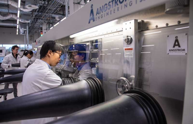
Angstrom Engineering® has engineered a platform that provides the photovoltaic and light emission communities a powerful tool for discovery and innovation using perovskite-based materials. The exceptional light absorption and charge transport properties of perovskites have made them an extremely attractive material set for solar cell research and development. Many of our partners are already working with this promising class of material in a variety of applications. The corrosive nature and high vapor pressure of many metal halides can create challenges for a vacuum deposition process. Angstrom Engineering® has implemented a set of unique process considerations within our platform, which — along with our built-in automation capabilities and unmatched customer support — will provide a path to breakthrough in this exciting field. Contamination Control - Most active perovskite layers are deposited using thermal evaporation, and many of these materials will present high vapor pressures at relatively low temperature. - These high vapor pressures can cause unwanted material to redeposit from coated chamber surfaces during elevated processing temperatures, leading to uncontrolled contamination. - Angstrom systems are equipped with extensive cooling solutions for sources, QCMs, shielding, and chamber walls to prevent material from redepositing and contaminating your process. With our carefully engineered cooling and shielding systems, you deposit only what you intend, where you intend it. Moisture Control - Moisture within the environment of a perovskite deposition chamber can negatively impact device performance and create corrosive byproducts, which can be damaging to hardware. - Angstrom provides a suite of solutions for removing moisture prior to – and during – deposition processes. - Cryogenic high vacuum pumps are excellent at removing water and are comprised of internal components that are non-moving and corrosion-resistant – all desirable properties for a perovskite-rich environment. - Internal and external chamber bake-out encourage adsorbed water on all critical surfaces into the gas phase where it can be easily captured by the vacuum pump. Atmospheric Control - Perovskite Series® deposition equipment chambers are most often paired with an inert environment glovebox system, providing users with an entire suite of capabilities that will enable the development of pure, repeatable perovskite devices. - Fundamentally, keeping the deposition chamber from contact with the atmosphere will keep its contents free of possible contamination, and our systems can easily accommodate this with a sliding chamber door from within the glovebox. - Due to the corrosive nature of perovskite materials and their byproducts, the internal surfaces of Perovskite Series® deposition equipment chambers are typically composed entirely of electropolished AISI (304 or 316) stainless steel.
CATEGORY
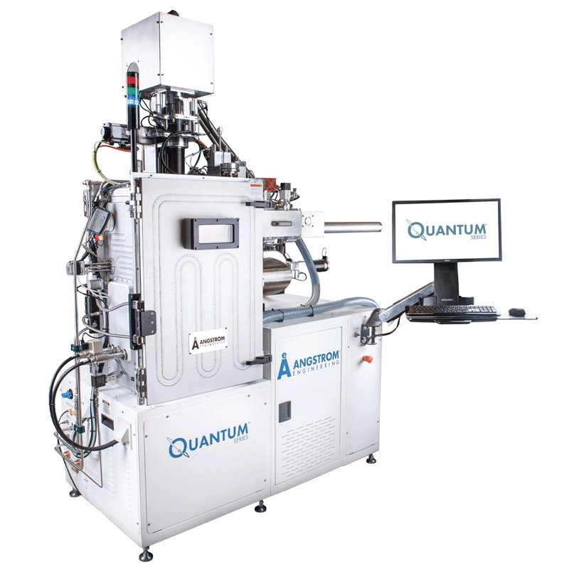
Angstrom Engineering® has developed a series of platforms that provide quantum computing hardware pioneers a means to reliably and confidently create superconducting circuits, and their supporting hardware, in a highly repeatable and automated framework. Next Generation Josephson Junctions Super Conducting Sputtering Indium Bumps The Quantum Series® of physical vapor deposition platforms cover a variety of fabrication processes vital in quantum computing research and commercial development. A Quantum Series® system can focus on one fabrication process or include several in situ. We regularly manufacture and deliver Quantum Series® systems specific to aluminum-based Josephson junctions, sputtering superconducting materials like niobium and tantalum, as well as systems dedicated to fabricating indium bump bonds. Process Specific Advantages Overview The Quantum Series® of physical vapor deposition platforms cover a variety of fabrication processes vital in quantum computing research and commercial development. A Quantum Series® system can focus on one fabrication process or include several in-situ. We regularly manufacture and deliver Quantum Series® systems specific to aluminum-based Josephson junctions, sputtering superconducting materials like niobium and tantalum, as well as systems dedicated to fabricating indium bump bonds. Grow Uniform Tunnel Junctions - The Quantum Series® Josephson junction fabrication platform employs a number of features to ensure repeatable growth of pure, uniform oxide layers. - We can accommodate static oxidation, dynamic oxidation, as well as plasma and UV/ozone oxidation. - We employ a robust gas purification system, real-time oxide growth monitoring, and direct optical wafer temperature monitoring allowing oxides that are customizable, repeatable, and reliable. Precise Shadow Evaporation - Angstrom has refined our design to create an extremely repeatable, versatile, and robust fixture. - Process enhancements are available, including substrate heating, cooling, and biasing. 3D Transmon Qubit The Josephson junctions our partners have fabricated measure up to established qubit benchmarks. These qubits were fabricated using Quantum Series® equipment and were independently characterized by the Institute for Quantum Computing (IQC) at the University of Waterloo, Ontario Canada.
CATEGORY
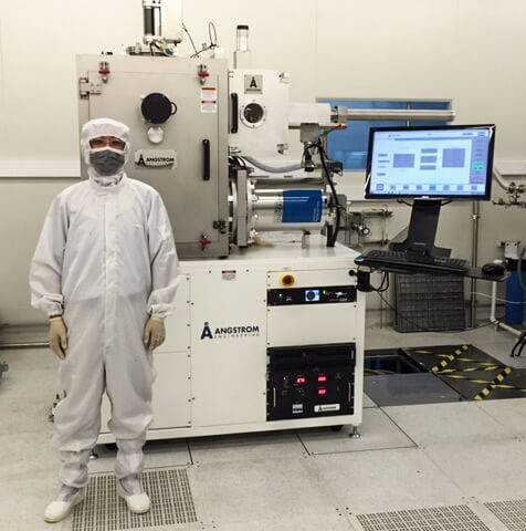
This device can be created with a wide range of superconducting materials, but aluminum is a common choice among researchers due to the relative ease of creating a high-quality oxide with it, as well as its relatively low melting point (660 °C), making it versatile. Josephson circuits are extremely sensitive to contaminants. - For this reason, evaporation and oxidization occur in independently sealed chambers, one for evaporation and one for oxidization. - Perfect isolation is achieved between the oxidization chamber and the deposition chamber using load-locks and programmable, recipe-driven automation through Aeres®, our advanced process control software. - Both chambers are constructed from electro-polished stainless steel to minimize off-gassing, and transfer between chambers occurs in situ to minimize venting. An e-beam source provides the best versatility for evaporating aluminum intended for superconducting circuits. - It allows for a higher volume of material and reduces the need to vent the chamber, further ensuring clean, contaminant-free films. - The vapor flux created by e-beam evaporation is ideal for patterning the fine features that Josephson circuits require. An ion source prepares the substrate for deposition with gentle cleaning or precision etching. Some materials used to create Josephson Junctions (such as Niobium) require the use of magnetron sputtering. A sputtering source can be seamlessly integrated into your thin film deposition platform. We create Josephson platforms that support multiple connected (though isolated) chambers for alternate deposition methods as well as analytical tools, all integrated into the overall process automation. This results in platforms of varying configurations, from dual chamber (deposition/load lock) to in-line systems, all the way to robotic radial cluster arrays incorporating deposition, oxidization, and analytical stations. Your system will be based on the type of junctions you plan to create as well as your specific throughput, material, and infrastructure requirements.
CATEGORY
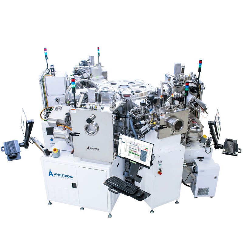
Angstrom’s pinnacle of automation, engineering precision, user control, and collaboration with you, our partner. These Nebula Cluster integrated vacuum systems are designed specifically to meet our client's process requirements. The number and type of vacuum modules are customer-selected and provide room for future expansion potential. Designed for the lab that requires a safe and reliable tool that produces repeatable, high-quality thin films in a compact footprint. We dream with you to determine the modules that will bring your potential innovations to reality. PVD, CVD, ALD, masking and parking transfer, stages with heating/cooling, sources that assist with cleaning, variable angle deposition and everything else current technology allows. Build Options The Nebula Cluster integrated vacuum system includes a centralized robotic hub connecting everything, all controlled with our integrated and simple-to-use recipe-driven software. Overview - Substrate cleaning and preparation using plasma or ion beam sources - Multiple vacuum deposition modules are available for PVD, CVD, ALD, & application focused modules, such as Quantum Series - Substrate and mask storage cassettes can accommodate 25 or more sample trays as needed - Distribution modules using SCARA robots are sized to meet your requirements - Glovebox environments can be integrated into one or more modules Substrate Size/Throughput - We have built modules that accommodate standard semiconductor wafer form factors, as well as typical display glass, including modules for Gen. 2 (360 mm x 465 mm) and larger. - Throughput depends on process duration and complexity. However, the AERES software platform optimizes layer-to-layer transitions to reduce overall process time. Nebula Cluster In The Field This integrated Nebula cluster system was installed at the University of Oxford's 'National Thin-Film Facility (NTCF) for Advanced Functional Materials' to support work in energy production. More here.
CATEGORY
