By Moorfield
Integrated deposition methods for air-sensitive thin-film materials and protected device workflows. Moorfield glovebox-compatible PVD systems help researchers keep sensitive materials under controlled atmosphere while retaining modular deposition capability. Platforms: MiniLab 026 / 090. Workflow: Protected transfer. Materials: Air-sensitive. Research-grade capability without enterprise complexity: This platform is positioned for research teams that need controllable thin-film process access, practical laboratory integration and clear configuration choices. Protected process transfer for oxygen and moisture-sensitive materials; Clear routing to MiniLab 026 and MiniLab 090 platforms; Sputtering and evaporation options by configuration; Strong fit for perovskites, OLEDs and sensitive interfaces; Configuration clarity for protected and standard lab workflows. Application-specific integration: For projects where atmosphere control defines the process approach. Glovebox interface discussion; Process and transfer planning; Application-led configuration. Key features: Modular research architecture - Configure sources, chambers, stages and monitoring around the research programme. Multi-technique capability - Combine sputtering, evaporation, e-beam and specialist process modules where required. Advanced process control - Support for recipe-led workflows, monitoring, gas handling and advanced power options. Scalable laboratory integration - Move beyond benchtop limits without defaulting to production-scale complexity. Application-specific options - Glovebox, load-lock, bias, heating and diagnostic options can be specified by project. Long-term adaptability - The system can be configured and expanded as research priorities evolve. Options and upgrades: Vacuum and transfer - Load-lock options; Glovebox compatibility where applicable; Dry pumping options; Process gas expansion. Sources and power - Magnetron sputtering; Thermal evaporation; E-beam evaporation; HiPIMS and pulsed DC options. Control and monitoring - Recipe-led operation; QCM rate/thickness monitoring; Substrate heating and rotation; Bias and diagnostic options. Technical specifications: System type - Glovebox-compatible PVD systems; Compatible platforms - MiniLab 026 and MiniLab 090; Best fit - Air-sensitive materials and protected device workflows; Processes - Sputtering and evaporation methods by configuration; Applications - Perovskites, OLEDs, organic electronics, PV and sensitive interfaces.
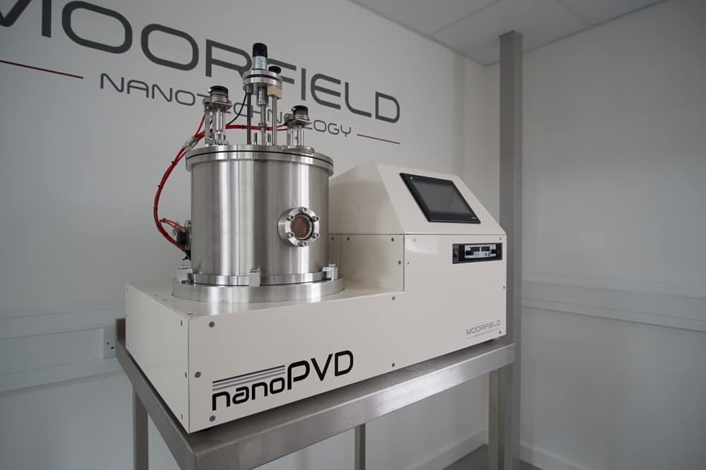
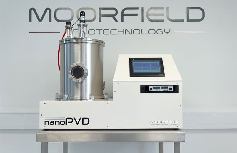
Benchtop PVD System Compact, research-grade RF/DC magnetron sputtering for advanced thin-film materials. The nanoPVD-S10A brings high-performance sputtering capability into a compact benchtop platform, supporting metals, oxides, nitrides, multilayers, and exploratory materials R&D. Substrates Up to 4" Base pressure <5E-07 mbar Sources Up to 3 magnetrons Research-grade sputtering in a compact benchtop platform The nanoPVD-S10A is compact enough for research laboratories and cleanrooms, while using high-end vacuum, source and control hardware for controlled thin-film deposition. It is optimised for RF and DC magnetron sputtering of metals and insulating materials, giving research teams a practical platform for repeatable materials development. - Compact footprint for research labs and cleanrooms - RF/DC compatibility for a broad material range - Configurable sources and gas handling - Recipe-driven operation via touchscreen HMI - Designed for serviceability and long-term use Benefits that matter in a working research lab Faster experimental cycles Keep early-stage sputtering work close to the research group, reduce waiting time and make process changes without competing for flagship cleanroom capacity. Ease of use for mixed-experience teams A touchscreen HMI, compact layout and straightforward maintenance help new users build confidence while still working on genuine research-grade sputtering processes. Research-grade flexibility RF and DC sputtering capability supports metals and insulating materials, including reactive and co-deposition methods for more advanced film stacks. Lower operational friction The benchtop format helps departments add local PVD capability without creating the access, facility and training burden associated with larger infrastructure. Better use of premium tools Develop and screen baseline recipes locally, then transfer mature work to larger shared systems only when the process is ready. Designed for real devices Useful for contact layers, seed films, functional coatings, TCO/dielectric studies, reactive sputtering and multi-material research workflows. Key features for thin-film process development Designed for laboratories that need repeatable sputtering capability without production-scale complexity. Compact benchtop design Advanced PVD capability in a space-efficient format for research labs, teaching spaces and cleanrooms. RF/DC magnetron sputtering DC sputtering for conductive materials and RF sputtering for conductive and non-conductive materials such as oxides and nitrides. High-vacuum performance Turbomolecular pumping supports low-contamination operation with base pressure below 5E-07 mbar. Reactive sputtering capability Gas and pressure control can support up to three process gases for oxide, nitride and compound film development. Recipe-based touchscreen control Touchscreen HMI with fully automatic operation and the ability to define and save multiple process recipes. Configurable source and gas options Up to three water-cooled magnetron sources for industry-standard 2" targets, with co-deposition and reactive process options. Typical nanoPVD-S10A configurations Start with a proven configuration, then tailor source, gas, stage and monitoring options around your materials and target films. Metals deposition For conductive films, contact metals, electrodes and exploratory materials work where reliable DC sputtering and practical geometry control matter. - Two magnetrons with DC power supply - SputterSwitch module for shared output - Substrate Z-shift and bi-shutter for best 4" substrate geometries - Quartz crystal sensor head for rate and thickness calibration TCO / dielectrics sputtering For transparent conductive oxides, dielectric coatings and process approaches that benefit from RF power and oxygen control. - Two magnetrons with RF power supply - SputterSwitch module for shared output - Substrate heating and additional oxygen process gas line - Substrate Z-shift, bi-shutter and quartz crystal sensor head Reactive / co-deposition For flexible materials R&D where researchers need source routing, multiple gases and mixed RF/DC process capability. - Three magnetrons with RF and DC power supplies - SputterSwitch for flexible power supply/source routing - Three process gases, for example argon, oxygen and nitrogen - Reactive deposition of oxides and nitrides Options and upgrades Configure the platform around the process approach, substrate handling, automation and laboratory services your application needs. Options are confirmed with quotation for the final build. Vacuum and gas handling - Dry backing pump - Fast chamber vent - Capacitance manometer and optional MFC closed-loop pressure control - Up to 3 MFC-controlled process gases Deposition and power - Up to 3 x 2" water-cooled magnetron sputtering sources - 780 W DC and/or 150 W, 13.56 MHz RF power supplies with auto-match - High-strength magnet pack for magnetic target sputtering - SputterSwitch source/power routing where specified - In-situ rate and thickness monitoring Substrate handling - Substrate heating up to 500°C; up to 600°C with 4-bulb configuration - Substrate cooling option - RF and DC substrate bias option - Rotation, Z-shift and shutters where specified Technical specifications Exact specifications depend on final configuration and should be confirmed with quotation. System type: Benchtop PVD / DC and RF magnetron sputtering Base pressure: 5×10⁻⁷ mbar Pressure control: Capacitance manometer + MFC closed-loop control as an option Process gas inlets: Up to 3 MFC-controlled gases Sputter sources: Up to 3 x 2" water-cooled magnetrons Target size: 2" Reactive sputtering: Yes; up to 3 MFCs with optional closed-loop control Magnetic target sputtering: High-strength magnet pack available Maximum substrate size: 4" (100 mm) Substrate heating: Up to 500°C optional; up to 600°C with 4-bulb configuration Substrate cooling: Available as an option Substrate bias: RF and DC bias available as an option Load lock: Not available as standard Glovebox compatible: No Process control: Industrial PLC + 7" HMI touchscreen Recipe control: Recipe save/load standard Footprint: 800 x 500 x 550 mm Warranty: 2 years Built for day-to-day usability The nanoPVD-S10A is designed to make advanced sputtering practical for busy research environments: quick to learn, straightforward to service and flexible enough to remain useful as research priorities evolve. - Comprehensive safety features - Touchscreen operation - Recipe storage - Easy servicing - Low running costs - Cleanroom compatible Frequently asked questions What is the maximum substrate size for the nanoPVD-S10A? The nanoPVD-S10A supports substrates up to 4 inches (100 mm) in diameter as standard. Can the nanoPVD-S10A sputter insulating materials? Yes. The system supports RF sputtering for non-conductive materials including oxides and nitrides, alongside DC sputtering for conductive targets. Is the nanoPVD-S10A compatible with glovebox transfer? No. The nanoPVD-S10A is not listed as glovebox compatible. For protected-transfer or air-sensitive workflows, contact Moorfield to discuss MiniLab glovebox-compatible configurations. What base pressure does the nanoPVD-S10A achieve? The system achieves a base pressure below 5E-07 mbar using turbomolecular pumping. Can multiple users run different recipes on the nanoPVD-S10A? Yes. The touchscreen HMI supports recipe save and load, allowing multiple users and projects to store and recall their own deposition parameters.
CATEGORY
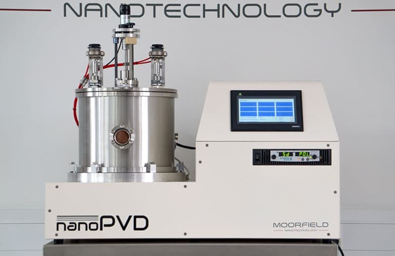
Wide-Area Benchtop PVD System Compact wide-area RF/DC magnetron sputtering for larger research substrates and coating areas. The nanoPVD-S10A-WA extends the compact nanoPVD sputtering workflow where standard 4 inch coverage is too restrictive, while keeping the system practical for research laboratories and cleanrooms. Substrate capability Up to 8 inch wide-area. Process RF/DC sputtering. Position Compact wide-area PVD. Research-grade capability without enterprise complexity This platform is positioned for research teams that need controllable thin-film process access, practical laboratory integration and clear configuration choices. - Wide-area sputtering without moving straight to a large modular system - RF/DC process flexibility for conductive and non-conductive materials - Configurable source, gas and pressure-control options - Recipe-led operation for repeatable research workflows - Designed for research labs, cleanrooms and process development Benefits that matter in a working research lab Faster wide-area coating cycles: Bring larger-substrate PVD experiments closer to the research team and iterate coating geometry, recipe settings and film properties without waiting for larger shared tools. Ease of use for mixed-experience teams: Touchscreen operation and recipe-led workflows support day-to-day use by researchers, students and technical teams working across changing projects. Wide-area research flexibility: The platform extends compact nanoPVD workflows where standard benchtop coverage is too restrictive, while retaining configurable RF/DC sputtering options. Lower operational friction: Add practical wide-area sputtering capability in a laboratory or cleanroom without the operational burden of production-scale equipment. Better use of premium tools: Screen larger-area films locally, then move validated processes to central facilities only when throughput, wafer scale or advanced integration requires it. Designed for device-relevant films: Useful for PV, sensors, optoelectronics, functional coatings, transparent conductive layers and larger-area materials-development samples. Typical configurations Use these examples as starting points. Moorfield can refine the final specification around your materials, substrates, gases, recipes and workflow constraints. Wide-area metals deposition: For contact metals, electrodes and seed layers where coating area matters. - RF/DC sputtering process - Larger substrate coverage than standard compact systems - Useful for device and coating R&D TCO and dielectrics: For transparent conductive oxides and insulating films that need controlled sputter conditions. - RF power option - Oxygen process gas options - Useful for PV, sensors and optoelectronics Functional coatings: For exploratory coating workflows where compact footprint and larger coating area both matter. - Research-friendly system scale - Recipe-led process access - Application-specific configuration Key features Compact laboratory footprint: Research-grade thin-film capability in a practical benchtop format. Configurable process approaches: Build around sputtering, evaporation or hybrid workflows depending on the model. Recipe-led control: Touchscreen HMI and recipe workflows improve day-to-day repeatability. High-vacuum platform: Turbomolecular pumping supports clean, controlled deposition conditions. Flexible gas and source options: Process gases, source count and monitoring options can be matched to the application. Research-first support: Moorfield helps specify the platform around your materials and target films. Options and upgrades Configure the platform around the process approach, substrate handling, automation and laboratory services your application needs. Options are confirmed with quotation for the final build. Vacuum and gas handling - Dry backing pump - Fast chamber vent - Capacitance manometer and optional MFC closed-loop pressure control - Up to 3 MFC-controlled process gases Deposition and power - Up to 2 x 2″ water-cooled magnetron sputtering sources - 780 W DC and/or 150 W, 13.56 MHz RF power supplies with auto-match - High-strength magnet pack for magnetic target sputtering - SputterSwitch source/power routing where specified - In-situ rate and thickness monitoring Substrate handling - Substrate heating up to 500°C - Substrate cooling option - RF and DC substrate bias option - Rotation, Z-shift and shutters where specified Technical specifications Exact specifications depend on final configuration and should be confirmed with quotation. System type: Wide-area benchtop PVD / DC and RF magnetron sputtering Base pressure: 5×10⁻⁷ mbar Pressure control: Capacitance manometer + MFC closed-loop control as an option Process gas inlets: Up to 3 MFC-controlled gases Sputter sources: Up to 2 x 2″ water-cooled magnetrons Target size: 2″ Reactive sputtering: Yes; up to 3 MFCs with optional closed-loop control Magnetic target sputtering: High-strength magnet pack available Maximum substrate size: 8″ (200 mm) Substrate heating: Up to 500°C optional Substrate cooling: Available as an option Substrate bias: RF and DC bias available as an option Load lock: Not available as standard Glovebox compatible: No Process control: Industrial PLC + 7″ HMI touchscreen Recipe control: Recipe save/load standard Warranty: 2 years Optimised for magnetron sputtering, the nanoPVD-S10A-WA is a Wide-Area configuration that extends the capabilities of the nanoPVD-S10A to allow for even coating of substrate diameters up to 8″, in a benchtop package. The wide-area version of the nanoPVD-S10A contains magnetron sputtering sources oriented directly upwards towards substrate platens. This arrangement in combination with substrate rotation and exposure plates with specially designed orifices allows for coating of substrates up to 8″ diameter for applications in which tight uniformity specifications are not critical. Like the nanoPVD-S10A, magnetrons are water-cooled for sustained high-power operation and accept industry-standard targets. In addition, nanoPVD-S10A-WA units come with all attractive features of the nanoPVD range including turbomolecular pumping systems, recipe-based automated operation via touchscreen HMIs, and compact designs for benchtop location. Key features - Benchtop configuration - Water-cooled magnetron sputtering sources for industry-standard 2″ targets - MFC-controlled process gases - DC and/or RF power supplies - Fully automatic operation via touchscreen HMI - Define/save multiple process recipes - Up to 8” diameter substrates - Base pressures <5 × 10⁻⁷ mbar - Equipped for easy servicing - Comprehensive safety features - Cleanroom compatible - Proven performance Options - Dry backing pump - Fast chamber vent - Automatic high-resolution pressure control - Additional process gases - 500 °C substrate heating stage - Substrate rotation, Z-shift and shutters - Up to 2 magnetron sputtering sources - RF and/or DC power supplies - SputterSwitch power supply/source switching technology - Co-deposition - Quartz crystal sensor head Typical configurations The nanoPVD-S10-WA is a semi-custom tool, with final design being subject to customer requirements. Service requirements All nanoPVD-S10A systems require chilled water, dry compressed air, nitrogen for venting (optional), process gas supplies, and electrical power. Exact requirements will be provided with quotations or on request.
CATEGORY
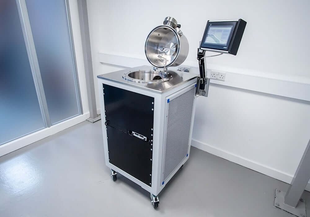
Benchtop Evaporation System Compact thermal and low-temperature evaporation for metals, organics and sensitive thin-film materials. The nanoPVD-T15A gives research teams local evaporation capability where controllable thermal and low-temperature workflows matter more than sputtering source count. Process Thermal / LTE Format Benchtop PVD Use case Sensitive materials The nanoPVD-T15A is a benchtop evaporation system optimised for deposition of various high-melting point metals and volatile organics. As compact as an electron microscopy coater, but with high-end hardware for research-grade results. Optimised for thermal evaporation onto substrates up to 4″ diameter. It can be equipped with standard resistive evaporation sources and/or low-temperature evaporation (LTE) sources for deposition of metals and organics, respectively. LTE sources are low thermal-mass for better control when evaporating volatile organic materials, while metals sources are our box-shielded TE1 models for efficient deposition and reduced cross-contamination. Chamber access is via a hinged lid that opens to reveal a stage suitable for holding substrates up to 4″ in diameter. The chamber is tall, allowing for high-uniformity coating via evaporative techniques. The units are easy to control via a touchscreen HMI interface, simple to maintain, have low running costs and come with a comprehensive range of safety features. With a turbomolecular pumping system, high-vacuum base pressures, straightforward automated control via a touchscreen HMI and a range of options for flexible configuration, the nanoPVD-T15A is a versatile, efficient solution for world-class R&D applications. Key features - Benchtop configuration - Organics and metals evaporation sources - High aspect-ratio chamber for uniform coating - Fully automatic operation via touchscreen HMI - Define/save multiple process recipes - Up to 4” diameter substrates - Base pressures <5 × 10⁻⁷ mbar - Equipped for easy servicing - Comprehensive safety features - Proven performance Options - Dry backing pump - Fast chamber vent - Up to 4 LTE sources for organics - Up to 2 evaporation sources for metals - 500 °C substrate heating stage - Substrate rotation, Z-shift and shutters - Quartz crystal sensor head Typical configurations Metals deposition: Two thermal evaporation sources for metals evaporation with shutters and quartz crystal sensor head for rate/thickness calibration. Organics deposition: Four LTE sources for organics deposition with shutters and quartz crystal sensor head for rate/thickness calibration. Metals and organics deposition: Two thermal evaporation sources and two LTE sources for metals and organics PVD, with shutters and quartz crystal sensor head. Service requirements All nanoPVD-T15A systems require chilled water, dry compressed air, nitrogen for venting (optional), and electrical power. Exact requirements will be provided with quotations or on request. Research-grade capability without enterprise complexity This platform is positioned for research teams that need controllable thin-film process access, practical laboratory integration and clear configuration choices. - Compact evaporation access for research laboratories - Thermal and low-temperature evaporation source configurations - Useful for metals, organics, electrodes and optical films - Recipe-led operation for repeatable development runs - Lower infrastructure burden than larger modular systems Benefits that matter in a working research lab Faster evaporation cycles Keep thermal evaporation of electrodes, contact layers and specialist materials close to the research group so early-stage process changes can happen quickly. Ease of use for mixed-experience teams A compact format, touchscreen HMI and recipe-based operation make the platform approachable for shared labs while preserving research-grade control. Research-grade evaporation flexibility Supports practical evaporation methods for metals, volatile organics and sensitive materials where local access and careful process development matter. Lower operational friction The benchtop format gives departments useful PVD capability without the access complexity, services load and training burden of larger infrastructure. Better use of premium tools Develop baseline evaporation recipes locally and reserve larger shared systems for mature processes, integrated runs or higher-capacity work. Designed for real devices Useful for electrodes, interfaces, organic electronics, quantum-device studies, small-batch coating work and proof-of-concept materials research. Typical configurations Use these examples as starting points. Moorfield can refine the final specification around your materials, substrates, gases, recipes and workflow constraints. Metals and electrodes For research teams depositing contact metals, electrodes and interfaces. - Thermal evaporation method - Compact local process access - Useful for device prototyping Low-temperature evaporation For volatile organics and sensitive materials that benefit from lower-temperature source configurations. - LTE source options - Sensitive material fit - Organic electronics and interface research Optical and functional films For exploratory coating work where deposition simplicity and clean workflow matter. - High-vacuum benchtop chamber - Recipe-led operation - Functional thin-film R&D Key features Compact laboratory footprint Research-grade thin-film capability in a practical benchtop format. Configurable process approaches Build around sputtering, evaporation or hybrid workflows depending on the model. Recipe-led control Touchscreen HMI and recipe workflows improve day-to-day repeatability. High-vacuum platform Turbomolecular pumping supports clean, controlled deposition conditions. Flexible gas and source options Process gases, source count and monitoring options can be matched to the application. Research-first support Moorfield helps specify the platform around your materials and target films. Options and upgrades Configure the platform around the process approach, substrate handling, automation and laboratory services your application needs. Options are confirmed with quotation for the final build. Vacuum and platform - Dry backing pump - Fast chamber vent - High-vacuum pumping approach for thermal evaporation - Recipe save/load operation Evaporation sources - Up to 4 LTE low-temperature evaporation sources - TE1 thermal evaporation source configuration - Source and shutter configuration for evaporation workflows - QCM rate/thickness monitoring where specified Substrate handling - Substrate heating up to 500°C - Substrate rotation where specified - Z-shift and shutters where specified - Up to 4" substrates Technical specifications Exact specifications depend on final configuration and should be confirmed with quotation. System type: Benchtop PVD / thermal and LTE evaporation Base pressure: 5×10⁻⁷ mbar Evaporation sources: Up to 4 LTE low-temperature evaporation sources Thermal evaporation: TE1 + LTE sources Maximum substrate size: 4" (100 mm) Substrate heating: Up to 500°C optional Glovebox compatible: No Warranty: 2 years Applications Published application-library examples and Bioz lookup results showing nanoPVD-T15A evaporation used for electrodes, organic and molecular films, sensors, energy devices and nanoscale spectroscopy workflows. Frequently asked questions What materials can be deposited using the nanoPVD-T15A? The nanoPVD-T15A supports thermal evaporation of metals, organics, and sensitive or low-melting-point materials that are not suited to sputtering. Is substrate heating available on the nanoPVD-T15A? Substrate heating options are available. Contact Moorfield to confirm temperature range and configuration for your specific application. Can the nanoPVD-T15A be used for organic semiconductor deposition? Yes. The low-temperature thermal evaporation approach makes it suitable for organic materials where sputtering plasma would damage the film or substrate.
CATEGORY
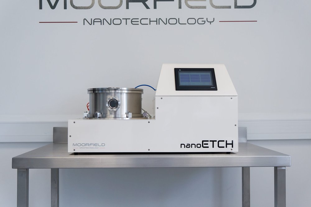
Compact plasma etching and surface modification for low-damage advanced materials research. nanoETCH is positioned for researchers who need controlled plasma processing for sensitive materials, device structures and early-stage process optimisation. Process: Plasma etch. Workflow: Low damage. Materials: 2D / semiconductor. Research-grade capability without enterprise complexity. The nanoETCH is positioned for research teams that need controllable thin-film process access, practical laboratory integration and clear configuration choices. - Controlled low-damage plasma processing for sensitive materials - Compact research access for etch and surface activation workflows - Useful for graphene, 2D materials and device fabrication - Recipe-led process development and repeatability - Practical alternative to tying up larger cleanroom tools Benefits that matter in a working research lab: Faster etch process cycles - Keep plasma etch development close to the research group, shorten feedback loops and make process changes without waiting for large shared cleanroom tools. Ease of use for mixed-experience teams - Touchscreen operation, recipe-led workflows and a compact footprint support daily use by researchers, students and process engineers. Low-damage research flexibility - Controlled plasma processing supports sensitive materials, graphene, 2D materials, surface activation and exploratory device-fabrication workflows. Lower operational friction - The compact research format helps labs add local etch and surface-processing capability without production-scale infrastructure or access constraints. Better use of premium tools - Develop and screen plasma recipes locally, then transfer mature work to larger cleanroom tools only when the process approach is ready. Designed for real devices - Useful for graphene patterning, 2D materials, semiconductor research, surface modification, nanomaterials and device-fabrication studies. Typical configurations: 2D materials etching - For low-damage workflows involving graphene and other sensitive materials. Controlled plasma processing; Research recipe development; Device structure fit. Surface activation - For preparing, modifying or activating surfaces during materials research. Surface modification method; Compact local process access; Repeatable development runs. Semiconductor etch R&D - For early-stage etch process screening and device fabrication workflows. Application-led process setup; Research lab integration; Cleanroom pressure relief. Key features: Dedicated process capability - Focused platform design for the target process rather than generic equipment messaging. Research workflow fit - Built for universities, R&D laboratories and pilot development environments. Controlled operation - Recipe-led controls and application-specific configuration improve repeatability. Compact laboratory integration - Add capability close to the research team without enterprise-scale infrastructure. Application-led specification - Moorfield can configure the system around materials, substrates and process objectives. Serviceable design - Designed for practical operation, maintenance and long-term research use. Options and upgrades: Process module - Application-led chamber configuration; Controlled process environment; Recipe-led operation; Compact laboratory integration. Automation - Touchscreen or PC/HMI operation; Recipe storage; Repeatable process sequences; User-focused controls. Research support - Configuration advice; Process development support; Serviceable system design; Clean laboratory integration. Technical specifications: System type: Precision plasma etching system Process type: Plasma etching and surface modification Best fit: 2D materials, semiconductor etching, surface activation and device fabrication Research value: Low-damage process development in a compact platform Applications: Graphene, nanomaterials, semiconductor R&D and surface engineering Applications: Application-library examples for nanoETCH and related plasma-process workflows in graphene, h-BN, SiO2, silicon and substrate-cleaning research. FAQ: What etch processes does the nanoETCH support? The nanoETCH supports RIE (reactive ion etching), plasma cleaning, surface activation, and selected fluorine-chemistry etching of materials including graphene, hBN, SiO2, and Si. Is the nanoETCH suitable for 2D materials? Yes. The system is specifically used for gentle plasma processing of sensitive 2D materials where shared etch tools designed for higher-power processes risk sample damage. What gases can be used in the nanoETCH? The nanoETCH supports argon, oxygen, and fluorine-based chemistries. Confirm your specific process gas requirements with Moorfield at the configuration stage. The nanoETCH is a benchtop etch tool with fluorine RIE and soft-etch capabilities. Unlock the full potential of reactive ion etching with our benchtop Nanoetch system—engineered specifically for high-performance fluorine-based RIE applications with soft-etch feature. Designed for advanced materials research, NanoEtch delivers industry-leading precision, uniformity, and process repeatability essential for today’s challenging etch requirements. Soft Etching: Soft Etching is the application of precisely-controlled low powers for etching applications involving highly sensitive materials (such as graphene or PPA thermal resist) or where ultra-low etch rates are needed. This allows for the routine use of plasma powers <5 W (down to 100 mW or below, subject to configuration and process), with up to 20 mW control resolution. An example application is the soft etching of very thin layers of thermal resist PPA. Heidelberg Instruments Nano utilise the soft etch feature in their high-resolution stack (lift-off/etching) using their market leading NanoFrazor Thermal Scanning Probe Lithography (t-SPL). They found that in a successful transfer process, it is important to reduce the PPA etch rate and the plasma ignition effect during the reactive ion etch step as much as possible. The soft etching capabilities of the nanoETCH allows reduction in the ignition effect to ~1 nm, opening doors to using even thinner layers of PPA (< 6nm) and further increasing the resolution and reliability of their NanoFrazor High-Resolution Stack processes. Fluorine-Chemistry Etching: For more aggressive reactive ion etch processes, nanoETCH systems can be configured for use with the fluorine-chemistry etchant gases SF6 or CHF3. For this, tools are equipped with a range of hardware and software enhancements. Recent applications of fluorine-chemistry nanoETCH tools have included: - h-BN sidewalls: A pit was etched into a multi-layer stack of h-BN, using Moorfield etching technology contained within a MiniLab 026. With SF6 as the etchant gas and a Soft Etching approach, just 7–8 layers of material were removed during a 2 minute process. Residual roughness at the bottom of the pt was just 1 atomic layer. - h-BN bulk etching: By changing conditions, much higher etch rates were possible. Users were able to achieve an etch depth of 130 nm at a rate of 1.1 nm/s. - SiO2 etching: A thermally oxidised Si wafer was etched using a nanoETCH tool using CHF3 as etchant gas. An ultra-low etch rate of ~1.3 Å/s was obtained, allowing for excellent control. - Si etching: Using SF6 and N2 it is possible to etch 25nm of Si in 20 seconds for applications such as HR stack layers. Key features: - Benchtop configuration - Soft-etching: Precision RF power <30 W - Up to 3 MFC-controlled process gases - Up to 6"/150 mm diameter stages - Fully automatic operation via touchscreen HMI - Define/save multiple process recipes - PC connection for data-logging - Base pressures <5 × 10⁻⁷mbar - Equipped for easy servicing - Comprehensive safety features - Cleanroom compatible - Proven performance
CATEGORY
