By Zyvex Labs
ZyVector is an STM control system which converts a scanning tunneling microscope into an automated STM lithography system. The system is controlled through our software package, Scanz, which allows for automation of almost every task, including Digital Vector Lithography. The software drives a 20-bit digital control box to handle the real-time control tasks such as the STM feedback loop and the creep and hysteresis correction which allows for precise tip positioning. This in drives high-voltage amplifiers to drive the STM piezo scanner. ZyVector is designed to connect to ScientaOmicron UHV STMs using the standard Omicron STM cabling. It can also be adapted to run other STM systems. Full System: Includes 20-bit Digital controller, Omicron Coarse Motion Controller, Piezo driver box, Scanz™ STM Lithography control software $195,000
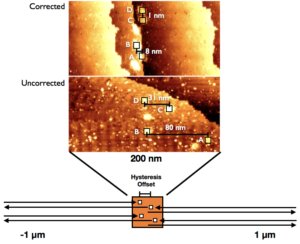
Unlike commercial STM systems designed for imaging, in ZyVector we wish to have the tip move arbitrarily across the surface with atomic precision. Therefore we must achieve real-time accuracy and precision in the tip position,so that STM images are undistorted, and lithography vectors follow their desired path. Piezo Creep and Hysterisis Correction Standard piezo actuators exhibit two types of position error: - Creep is a time-dependent error, whereby the last 10% of any motion does not happen instantaneously, but occurs over tens or hundreds of seconds. - Hysterisis is a position-dependent error; if the tip moves away from zero, and then back again, the tip will not return to the original location. The 20-bit controller in Zyvector adjusts the voltages delivered to the piezo actuators in order to correct these errors in real time, giving accurate and precise tip positioning. Corrections are applied to all four quadrants of the piezo tube, and therefore motions in x, y and z are all corrected. Piezoelectric elements used in commercial STM systems suffer from time-dependent errors called creep.In typical commercial STM control systems, this creep goes uncorrected, because for typically imaging tasks, a distortedimage is good enough. The offset between the forward andbackward scan while imaging is also due to creep. In ZyVector, we correct these creep errors in real time. First, the creep characteristics of each piezo scanner must be calibrated.A large jump is made, and then the tip scans a single linescan repeatedly. As the tip position creeps, the position of thedimer rows dri s, in a curve. The curvature of the dimer rows is parameterized, and used to correct the motion of the piezo scanner. First 200 s after 500 nm jump (Uncorrected Creep vs. Creep Corrected) Distortion-free Imaging Creep also occurs on a millisecond timescale, and causes an offset between the forward and backward scans. This means that the tip is never really where it appears to be. With creep correction applied, the forward and backward scans overlap exactly, making precise tip positioning over a dimer row or other feature possible. Distortion Free Imaging (Creep Correction Off vs. Creep Correction On) The effect of Creep on Lithography Precision We use test lithography patterns to measure the effectiveness of the creep correction. The test pattern shown is a set of concentric boxes, which is defined using two bitmaps, one for the left half of the pattern, and one for the right half. Without creep correction, the rectangles are not concentric, are not square, and the pairs of lines are not adjacent. There is also an offset between the two half patterns. By running this and other test patterns, repeated many times, we can obtain quantitative data for the precision of the motion. The table shown below gives the precision of the tip motion for two different systems, after 10 repetitions of the test patterns. For larger motions, Scanz can use a c ombination of real-time creep and hysteresis correction, and alignment to surface fiducial marks to maintain accurate positioning. Accurate navigation across the surface with creep and hysteresis correction. For larger motions, Scanz can use a combination of real-time correction of creep and hysteresis, and alignment to surface fiducial marks to maintain accurate positioning while making large jumps across the surface. Testing Hysteresis Correction: In this test, the tip makes large jumps back and forth, and draws a box after a rightwards jump, and then after a leftwards jump, as indicated by the arrows. The hysteresis offset is measured as the distance between the second and third boxes. This offset is then put into Scanz, to correct the hysteresis. Results of a hysteresis test script. The hysteresis is measured from the distance between the 2nd and 3rd boxes of each set. Uncorrected: In the first set of boxes, the distance between boxes after a 1 μm jump is 80 nm, which is a mixture of creep and hysteresis. In the second set, the tip waited a few minutes before drawing a box, and the offset is now 30 nm, which is mainly hysteresis. Corrected: A similar data set after applying creep and hysteresis correction. Now the boxes are all almost perfectly aligned,even after a 1μm jump. Automated Fiducial Mark Alignment Over larger distances, effects such as thermal drift and uncorrected creep and hysteresis can still cause errors in the tip position. With STM, the surface can be imaged without affecting the H layer, using the same probe as for writing. This allows for direct alignment to a previously written pattern, or to a deliberately written fiducial mark. A series of scripts are provided in Scanz, giving the capability to search for, identify, and automatically align to fiducial marks on the surface, so that accumulated position errors can be zeroed. In this way, residual position errors can be minimized. A fiducial mark is located, by comparison to a previous image of the mark t aken after writing. The scan centre is relocated to the fiducial mark,even using low resolution, fast imaging. Lithography Test Pattern (Creep Correction Off vs. Creep Correction On) ZyVector has great flexibility in the methods for pattern definition; either as geometric shapes, or as arbitrary bitmaps. There is a special script, MultimodeVectorGen, which reads bitmaps and writes them out as patterns.
CATEGORY
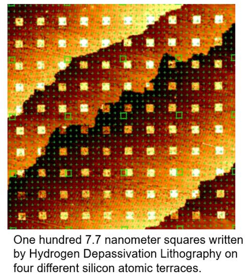
Zyvex Litho 1™ Sub-nm Resolution Lithography System View brochure here Making Atomic Precision Lithography a Reality - UHV system for STM Lithography - Precursor Gas Dosing and Si MBE - Digital Vector Lithography - Automation and Scripting This exposure of 7.7nm (10 pixel) squares would not be possible without sub-nm resolution and precision. Technical Specifications: ZyVector Lithography Controller - 20-bit DSP - Provides real-time control of the tunneling feedback loop and bias voltage. and precise tip motion across the surface. - Piezo Driver - Pre-amp bias range control for Omicron preamp amplified current input Fits Omicron VT STM preamp and PIC cabling. Scanning - Omicron VT STM: 9500 nm. - Minimum scan bit size: 10 pm. - Z range: 1.3 μm. - Minimum bit size: 1 pm. System Capabilities - Heater station for Sample Preparation - Si MBE source - Precursor gas dosing chambers Advanced Position Controls - Local piezo tube calibration based on lattice recognition, including determination of lattice angle relative to piezo tube axes. - Lattice phase recognition for precise lithography positioning. - Creep and Hysteresis position correction (CHC) in xyz. - Initial optimization of creep and hysteresis over scan range during installation. (Fine optimization by user required periodically.) Hydrogen Depassivation Lithography (HDL) - Two spot size modes available: - AP mode ( single-dimer-row line width) - FE mode ( wide line width, rough edges) Advanced Scripting Capabilities - We provide scripts based on Python for test HDL patterns, creep correction calibration, lithography parameter calibration, etc. - User-written scripts can be easily incorporated and run using command line interface or drop-down menu.
CATEGORY
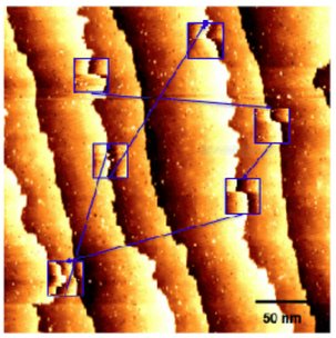
A new leap forward in STM design: real-time position correction The ZyVector STM control system from Zyvex Labs uses live position correction to enable atomic-precision STM lithography. Now the same live position correction technology is brought to STM microscopy and spectroscopy users, enabling fast settling times after large movements in xy and z, and precise motion across the surface, landing and remaining at the desired location. Capabilities: - Removal of creep-related xy and z drift – Rapid tip settling for slow IV curves. - Remove image distortions – no forward/backward scan offset, correct dimensions. - Accurate navigation across the surface – 10 nm error on 5 µm jump. - Jump precisely to point of interest for imaging or spectroscopy. - Real-time correction of creep and hysteresis behind the scenes, without modification. The CHC box receives the piezo voltages from the digital controller, modifies them to correct for creep and hysteresis, and then passes the corrected voltages on to the piezo drivers. In this way, the corrections are achieved without any required modification of the STM control system.
CATEGORY
