3D scaffold platform for neuronal network development is currently produced by laser-based microfabrication method, 2-Photon Polymerisation (2PP). The application of the 2PP microfabrication technology for 3D structure fabrication offers unique possibilities in controlling structure resolution, design complexity, and reproducibility. Up to date, 2PP technique is the only method capable of manufacturing of consistently reproducible complex 3D scaffolds with a very high structure resolution. The developed technological process chain for 3D incorporation of microelectrodes allows the creation of a novel biotech product – 3D polymer scaffold platform with integrated electrodes for neuronal network development and characterisation. The functional reproducibility of such networks allows researchers and pharmaceuticals to test compounds/interventions that modulate network activity enabling, for the first time, in vitro human testing at the functional level. The commercially available scaffold platforms from Laser nanoFab will provide a high throughput tool for screening novel drugs and compounds that may impact upon the disease process and expedite the process of drug development. The Launchpad “Scaffold-Needs” project will aim to make 3D scaffolds and 3D scaffold platforms with integrated electrodes commercially available via the young start-up German company Laser nanoFab GmbH. It is envisaged that the 3D scaffold platforms will enable scientific and medical researchers to use them for a variety of studies e.g. as 3D neuronal cell models for investigations of fundamental mechanisms of human neuronal activity; in tests of pharmacological and toxicological compounds, in modelling of neuronal diseases, etc. One of the aims of MESO-BRAIN project is to develop unique biocompatible 3D platform with integrated electrodes that can be fabricated on a large scale and in reproducible manner. First prototype 3D scaffold platform concepts designed by Aston University have been already fabricated and tested in the frame of the MESO-BRAIN project.
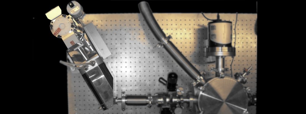
The EUV tube provided by Laser nanoFab GmbH is a compact and user-friendly extreme ultraviolet (EUV) source for metrology. The source is based on advanced microfocus X-ray tube technology that has been extended to the EUV spectral range. The EUV emission is generated by electrons colliding with solid state targets. This concept guarantees debris-free operation, well-defined performance characteristics and excellent long-term temporal and spatial stability. EUV POWER At present, EUV powers of up to 20 μW (2π sr, 2% bw) are achieved. STABILITY The EUV source has excellent long-term stability. In continuous operation the fluctuations were measured over a period of three days and typically less than 1%. SOURCE SIZE The source size is below 10 µm and can be varied via operation voltage and current. Source sizes of 100 μm and more are possible (full width at half-maximum). INTERFACE The EUV tube comes with a standard vacuum flange, so connection to your vacuum setup is easy. The EUV emission cone is centered on the flange axis. OPEN DESIGN Customer-specific adaptations are possible. APPLICATIONS - At-wavelength characterization of EUV optical components, e.g. multilayer mirrors, masks, or filters - Off-synchrotron calibration of EUV tools, e.g. spectrographs and energy monitors - EUV imaging and microscopy with high lateral resolution KEY FACTS - Compact set-up, easy and intuitive operation - Debris-free operation - Excellent long-term temporal and spatial stability - Very low running costs - Computer-controlled (start-up, centering, focusing, operation)
CATEGORY
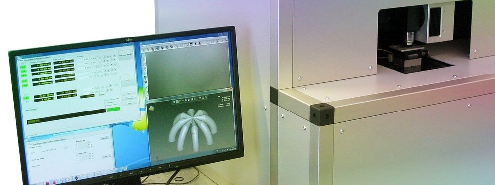
Direct laser writing by two-photon polymerization (2PP) of photoresists is an emerging technique for the fast and flexible fabrication of fully three-dimensional (3D) structures with structure sizes down to less than 100 nm. The M4D micro- and nanostructuring system enables high-speed generation of 2D and 3D micro- and nanostructures over large areas and volumes. Applications - Microfludics - Biology - Medicine - Microoptics - Micromechanics - 3D Free-form structuring - 2D Surface structuring TECHNOLOGIES - Polymerization of photoresists with femtosecond laser - Submicrometer resolution with two-photon polymerization - Micro- and nanostructuring MATERIALIEN - Our optimized photoresists for 2PP: femtoBond ® - Standard photoresists for lithography - Biodegradable and biocompatible photoresists FAKTEN - Rapid Prototyping from Nanometer to Millimeter - Key technology for 3D nano rapid prototyping - For research and development PARAMETERS Resolution 100nm – 100µm Positioning Speed (typical) up to 50 mm/s Scanning Speed (typical) up tp 1 m/s Polymerization Volume (typical) 10cm x 10cm x 10cm Lasertypes Ultrashort Lasers System Open Design, customer specific modifications possible Footprint ca. 1 m² Configuration example femtosecond pump laser wavelength 1030nm pump laser power 10W pump laser rep. rate 1kHz to 1 MHz pump laser pulse duration 290 fs-10 ps second harmonic generator: laser output power 0.7 W pulse duration < 100 fs wavelength 515 nm repetition rate 75 MHz ± 1 linear axes air-bearing bidirectional repeatibility < ±0,075 µm speed (w/o load) (XY) 2m/s, (Z) 1m/s objective NA 0.5 2PP-structure height (Z) WOW-2PP prepared, structure height in Z only limited by the travel of the Z-axis software can be extended with own Visual Studio modules Other configurations are available.
CATEGORY
The EUV tube provided by Laser nanoFab GmbH is a compact and user-friendly extreme ultraviolet (EUV) source for metrology. The source is based on advanced microfocus X-ray tube technology that has been extended to the EUV spectral range. The EUV emission is generated by electrons colliding with solid state targets. This concept guarantees debris-free operation, well-defined performance characteristics and excellent long-term temporal and spatial stability. The characterization and quality control of multilayer mirrors, masks and optical components for the extreme ultraviolet lithography requires a compact, stable and debris-free light source. Laser nanoFab GmbH offers such a light source for metrology, which is based on the electron-induced characteristic emission of solid targets. Applications - At-wavelength characterization of EUV optical components, e.g. multilayer mirrors, masks, or filters - Off-synchrotron calibration of EUV tools, e.g. spectrographs and energy monitors - EUV imaging and microscopy with high lateral resolution
CATEGORY
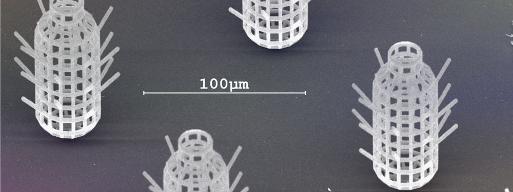
femto Bond ® is our line of unique photoresists designed for 2D and 3D lithography techniques such as two-photon polymerization (2PP). femto Bond ® 4B...is our proven photoresist for use with near-infrared lasers e.g. around 800 nm. femto Bond ® 4C...is our proven photoresist for use with near-infrared lasers e.g. around 520 nm. Vorteile - Negative photoresist - Highest resolution - Easy handling - Robust processing - Very low shrinkage - Biocompatible - Transparent in polymerized state - True 2PP resist, hardly affected by daylight - Organic-inorganic hybrid material
CATEGORY
