By ACST, Advanced Creative Solutions Technology, LLC
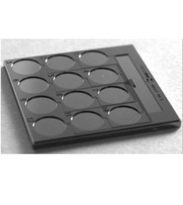
The Reservoir chips are ~1 cm², and fit easily onto the sample puck and stage of the DPN 5000, NSCRIPTOR™ and NLP 2000 systems. Universal reservoir chip have six (6)reservoirs and two (2)different channel configurations, corresponding to different pen types. The reservoirs are filled with solution using a micropipette. Use of several reservoirs allows the probe arrays to be coated with the same or different inks depending on the probe and Reservoir chosen. Manufacturer Name:NANOINK SKU: R-0001
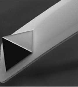
These probes are designed for contact imaging on soft material. Thanks to their ultra-small diamond structure, their surfaces are extremely smooth and exhibit low friction, yet they retain the extreme wear and chemical resistance and inertness, which is critical when imaging soft material. Here are the properties of these tips: - Scanning soft and hard surfaces in contact mode - Quality control - Long tip life time - Bio friendly due to its low surface energy which leads to superior imaging performance on soft, sticky samples such as protein, polymers, DNA, viruses, bacteria and cells - Resist fouling and build-up of debris when imaging soft material - Low friction which inhibits sample damage during imaging Product Description NaDiaProbes are all-diamond probes for advanced AFM-based research. These probes are not diamond coated or diamond-like carbon. In NaDiaProbes both the cantilever and probe tip are made of UNCD® (Ultrananocrystalline Diamond) a patented diamond thin-film made to a monolithic structure. Some Unique UNCD material properties are: - Mechanical Properties: Equivalent to natural diamond in hardness, Young’s modulus, fracture toughness and strength. - Tribological Properties: Smooth UNCD exhibits friction coefficients as low as 0.03 in air. - Transport Properties: Some UNCD films exhibit some of the highest conductivity reported for a phase-pure diamond film and are more conductive than any doped crystalline diamond film or diamond-like carbon film. - Electron Field Emission Properties: UNCD films consistently exhibit very low threshold fields for field electron emission. Emission currents as high as 100 µA from a single UNCD-coated silicon micro-tip have been observed. Emission currents as high as 1 mA have been achieved from conformally-coated arrays of silicon microtips. NaDiaProbes have been used for different type of applications ranging from imaging to nanoindentation. NadiaProbes are designed to fit most commercial AFM instruments. Additional Information Type: CTIT2L, CTIT2S Sharpness: Regular Quantity: Pack of 50
CATEGORY
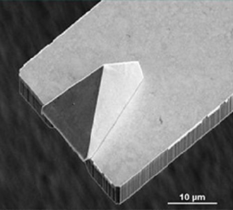
Data Sheet These probes are designed for Scanning Spreading Resistance Microscopy (SSRM) which enables simultaneous topographic imaging and 2D carrier density mapping on the surface of semiconductor samples. In addition these probes can be used for nano-indentation and nano-scratching applications. These probes can be used for imaging in contact mode, in air, liquid, on hard surfaces and non-contact mode. Here are the properties of these tips: - Extreme hardness, for indenting many surfaces - Extreme wear resistance, no change after many scans - Extremely strong, as strong as a single-crystal diamond - Very low friction, coefficients of friction 0.03 in air - Low stickiness, Hydrophobic surface NaDiaProbes are all-diamond probes for advanced AFM-based research. These probes are not diamond coated or diamond-like carbon. In NaDiaProbes both the cantilever and probe tip are made of UNCD® (Ultrananocrystalline Diamond) a patented diamond thin-film made to a monolithic structure. Some Unique UNCD material properties are: - Mechanical Properties: Equivalent to natural diamond in hardness, Young’s modulus, fracture toughness and strength. - Tribological Properties: Smooth UNCD exhibits friction coefficients as low as 0.03 in air. - Transport Properties: Some of UNCD films exhibit some of the highest conductivity reported for a phase-pure diamond film and are more conductive than any doped crystalline diamond film or diamond-like carbon film. - Electron Field Emission Properties: UNCD films consistently exhibit very low threshold fields for field electron emission. Emission currents as high as 100 µA from a single UNCD-coated silicon micro-tip have been observed. Emission currents as high as 1 mA have been achieved from conformally-coated arrays of silicon microtips. NaDiaProbes have been used for different type of applications ranging from imaging to nanoindentation. NadiaProbes are designed to fit most commercial AFM instruments. Additional Information Type: SSCRL, SSCRS Sharpness: Regular, Sharp Quantity: Pack of 5, Pack of 50
CATEGORY
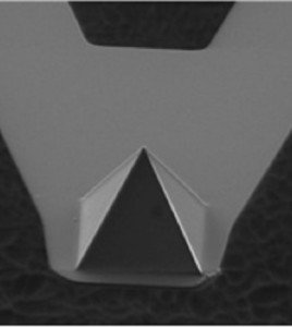
From: $950.00 Data Sheet These probes are designed for conducting scanning probe microscopy (C-AFM), Oxidation lithography, E-Chem AFM, Piezo-Force microscopy and SSRM. These probes feature high electrical conductivity and they are not like the metal coated probes. These probes are totally conductive. Additionally, the apex of less than 10 nm radius is respectively sharp when compared to the metal coated probes which gives unprecedented topographic and electrical resolution. Here are the properties of these tips: - No tip wear/Extremely durable - No tip shape degradation - Low friction - Suitable for bio-applications - Enables unparalleled resolution NaDiaProbes are all-diamond probes for advanced AFM-based research. These probes are not diamond coated or diamond-like carbon. In NaDiaProbes both the cantilever and probe tip are made of UNCD® (Ultrananocrystalline Diamond) a patented diamond thin-film made to a monolithic structure. Some Unique UNCD material properties are: Mechanical Properties: Equivalent to natural diamond in hardness, Young's modulus, fracture toughness and strength. Tribological Properties: Smooth UNCD exhibits friction coefficients as low as 0.03 in air. Transport Properties: Some of UNCD films exhibit some of the highest conductivity reported for a phase-pure diamond film and are more conductive than any doped crystalline diamond film or diamond-like carbon film. Electron Field Emission Properties: UNCD films consistently exhibit very low threshold fields for field electron emission. Emission currents as high as 100 µA from a single UNCD-coated silicon micro-tip have been observed. Emission currents as high as 1 mA have been achieved from conformally-coated arrays of silicon microtips. NaDiaProbes have been used for different type of applications ranging from imaging to nanoindentation. NadiaProbes are designed to fit most commercial AFM instruments. Additional Information Type: CTCR1L, CTCR1M, CTCR1S, CTCT2L, CTCT2S Sharpness: Regular, Sharp Quantity: Pack of 5, Pack of 50
CATEGORY
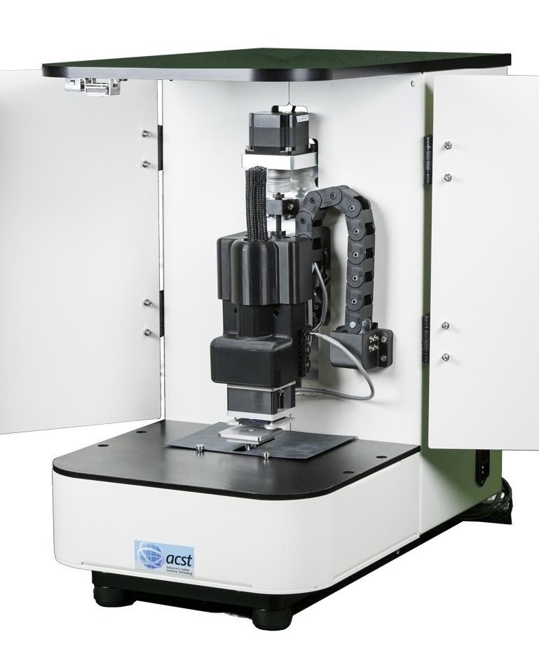
Finally, one nano fabrication tool that can do so much more!! ACST brings to researchers and educators one of its kind, an advanced and multi-purpose desktop micro and nanofabrication instrument that can serve as a research and education too. While it will allow researchers to take their existing work in different directions, it will enable educators to lay a strong foundation for students to master industrially useful micron and nano fabrication techniques. COSMOS nanoFAB is a fabrication platform, and is essential to our nano-SCIENTIST™ educational program that prepares students for the abundant opportunities in the growing field of microfabrication and Nanotechnology. COSMOS nanoFAB is designed with a very thoughtful approach to performance, cost, and versatility. Its modular design concept allows use of the common mechanical/electrical components across different techniques resulting in ease of use and lower cost. Additionally, the modular and flexible concept allows use of future modules under development, further improving the capability and ROI. The equipment consists of a solid foundation and very accurate XYZ stages are equipped with stepper motors coupled with encoders for fine control. It comes ready with a very sensitive load cell that allows for detecting contact with the sample and controlled application of load in relevant techniques. While the instrument is fully capable of being a research tool for rapid prototyping or experimental validation of new research, in the world of education, COSMOS nanoFAB will enforce teaching and application of concepts in surface chemistry, material science, industrial applications, electronic components, semiconductors devices, bio immobilization, and bio-sensing applications. Module 1 - Photolithography: Through a series of experiments, students learn the concepts and critical parameters of Photolithography: current foundation of the semiconductor industry. - Micro-Contact Printing (µCP): Researchers could use to make prototype samples or Educators can get class acquainted with one of the oldest and lab friendly technique to pattern nano & micro scale features of organic, inorganic and bio materials. - Photo NanoImprint Lithography (UV-NIL): A great technique for researchers to pattern and fabricate at the nano scale, thus opening new possibilities for their existing research. On the education front, students can experience and practice NanoImprint Lithography, considered by industry experts as the most promising technique that will meet the future demands of the semiconductor industry.
CATEGORY
