By Eulitha AG
PhableR TM R&D and Low Volume Manufacturing of Photonic Patterns ACADEMIC Nano Optics Nano Materials Plasmonics Research & Development XR ARVRMR Near-Eye Waveguides Head-up Displays (HUD) OPTOELECTRONICS DFB/DBR Lasers VCSEL Polarizer Gratings PCSEL Photonic Crystals Nanowire Devices PHOTORESIST SUPPLIERS Material Quality Testing Photoresist R&D OPTICAL COMPONENTS Telecom Gratings Anti-Reflective Surfaces Laser Diffraction Gratings Spectrometer Gratings Wire Grid (Polarizer) BIO MEDICAL Bio Molecular Sensors X-Ray Imaging COLORVISUAL EFFECT Structural Colors Security Applications • Photolithography system for low volume and R&D. • Non-contact: protects masks and substrates from damage and contamination • Highly uniform and reproducible printing • 1D and 2D periodic pattern printing • Suitable for non-flat substrates • Suitable for thin glass substrates • High Resolution: <65nm or 125nm (minimum half pitch for UV and DUV versions) • Overlay alignment capability • Works with commercially available masks and photoresists • Application support: Photoresists, Masks • Low maintenance and production costs LITHOGRAPHY FOR PHOTONICS Applications PATTERN EXAMPLES UV <125nm half-pitch 100mm, 150mm, larger size on request 6” <3% >1μm Manual load – automatic exposure <1μm frontside, manual 105mm, 155mm, 205mm DUV <65nm half-pitch >0.1μm Minimum CD (linear grating) Wafer size Mask format Illumination uniformity Resist thickness Operation Overlay alignment Beam size SPECIFICATIONS The PhableR tool provides an unprecedented ability to print high resolution periodic structures in a low cost tabletop photolithography system, ideal for small volume, academic, and R&D applications requiring a high degree of flexibility. Structures such as submicron period linear gratings and 2D patterns including hexagonal and square lattices are printed with high uniformity and fidelity. > Hexagonal hole array 600nm pitch Linear grating 300nm pitch Hexagonal pillar array 600nm pitch Square hole array 350nm pitch Hexagonal pillar array 3000nm pitch Square pillar array 300nm pitch
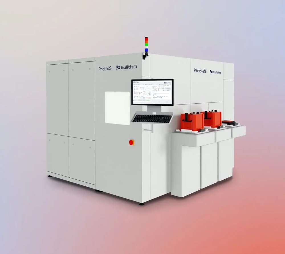
Step-and-repeat lithography system The PhableS is a step-and-repeat lithography tool designed for larger wafer sizes, such as 200 mm, 300 mm, and beyond. Using the large exposure fields of displacement Talbot lithography (DTL), the PhableS tool can fill larger substrates with multiple exposures. This tool is equipped with automated wafer and mask handling within a particle-controlled environment, ideal for high-volume industrial production. It features a variable exposure field size, allowing selective printing across multiple device masks. Specifications - Resolution (linear grating): UV <125 nm half-pitch; DUV <65 nm half-pitch - Wafer size: 300 mm; larger size on request - Mask format: 6″ - Illumination uniformity: <3% - Resist thickness: UV 1 µm; DUV 0.1 µm - Operation: Automated wafer and mask handling, factory interface compatible - Overlay alignment: <1 µm frontside, < 5µm backside - Duty cycle control: Variable compatible; At 150 nm pitch: 0.4 to 0.65 DC At 300 nm pitch: 0.3 to 0.75 DC - Throughput: 40 WPH - Maximum Exposure Field Size: 140 mm x 140 mm
CATEGORY
Pattern Period: 800nm, 1000nm, 1200nm, 1500nm; Pattern Area: 20x20mm² square each; Linewidth: 400nm/800nm, 500nm/1000nm, 600nm/1200nm, 700nm/1500nm; Max. Feature Height (Si / Fused Silica): <1000nm / <500nm
CATEGORY
Pattern Period: 300nm, 400nm, 500nm, 600nm; Pattern Area: 10x10mm² square each; Linewidth: 135nm/300nm, 175nm/400nm, 250nm/500nm, 300nm/600nm; Max. Feature Height (Si / Fused Silica): <300nm / <150nm
CATEGORY
