By Aixtron Se
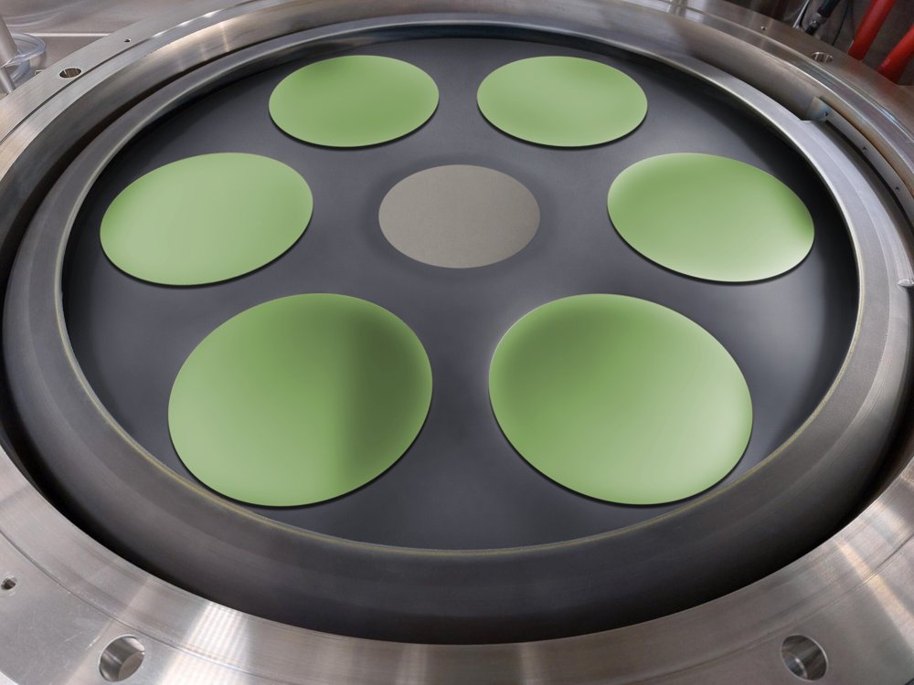
150/200 mm high throughput epitaxy for SiC Power Electronics Dual wafer size batch reactor G10-SiC - 150 mm and 200 mm – dual wafer size capable – safeguard your investment into the future - Highest wafer output / m 2 in the market - Lowest cost / wafer in the market - Excellent run-to-run process performance - Highly uniform, low defect SiC epitaxy processes for maximum chip yield Planetary Reactor® for 9 x 150 mm & 6 x 200 mm Your benefits - Single wafer performance in batch configuration - Best in class productivity - Best in class epi cost Our solutions - Fully automated wafer loading (C2C) - Individual wafer Gas Foil Rotation (GFR) - Automated Top side wafer Temperature Control (TTC) for optimized batch processing - Largest reactor capacity (9 x 150 mm & 6 x 200 mm) - High growth rate SiC processes - Hot wafer transfer and fast thermal reactor cycling - Best in class wafer throughput per m2 fab space efficacy - Low consumable cost per wafer - Highest efficiency in gas & power consumption per wafer G10-SiC: 200 mm uniformity G10-SiC: 150 mm uniformity
150/200 mm high throughput epitaxy for GaN power & RF applications . Our product for 150/200 mm GaN epitaxy G10-GaN - Highest wafer/m² fab area 3 process chamber compact cluster design with 50 % footprint reduction - Best in class device yield 3x on-wafer uniformity improvement at lowest particle level for all wafers (within run, run-to-run, chamber-to-chamber) - Lowest epi cost/wafer in the market 25% lower epi cost than any other platform Planetary Reactor® Your benefits - Highest wafer yield Low particle density (~0.1/cm²) Excellent uniformity (on-wafer, wafer-to-wafer) - Best in class productivity Outstanding reproducibility ≥90 % equipment uptime - Best in class epi cost Highest throughput/m² fab Lowest labor & chemical cost Our solutions - Fully automated wafer handling (C2C) - Novel wafer carrier design - Individual wafer close loop topside temp. control - Individual control of thickness & composition uniformity by 5-flow injector - Automated chamber cleaning - Long lifetime consumables - Smart system with predictive functionalities - Advanced chamber-to-chamber matching capabilities - Large capacity batch Planetary Reactor® - Compact cluster design with 3 process chambers - Highest chemical efficiency by 5-flow injector - Lowest operator assistance due to 50 wafer capacity on C2C The best of both worlds Single wafer performance at lowest batch processing cost Composition uniformity On-wafer device uniformity (650V application) G10-GaN enables seamless process transfer from today's tool of record AIX G5+ C - Same cassette-to-cassette wafer handling - „On-board“ calibration and control modes for process matching - Identical process chamber size and wafer configuration High productivity MOCVD solution for 150/200 mm GaN power & RF applications
CATEGORY
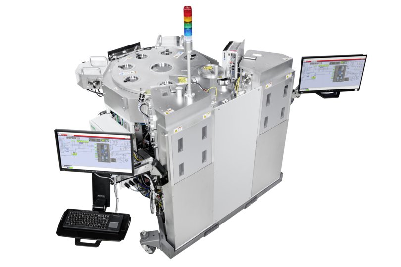
The Enabling MOCVD Solution Fully Automated MOCVD for High Volume Production of GaAs/InP Materials Cassette-to-Cassette Wafer Handling - Fully automated loading of wafers - Compatible with current and future wafer sizes 75 mm | 100 mm | 150 mm | 200 mm | optional SMIF port - Vacuum cassette elevators for 2 x 25 wafer cassettes - Clean environment for lowest defect levels - Significant reduction of labor cost – both on operator and expert level Fully Automated MOCVD for High Volume Production of GaAs/InP Materials Market Opportunity - Future proof - Compatible with current and future wafer sizes 75 mm | 100 mm | 150 mm | 200 mm | optional SMIF port - Highest uniformity and repeatability – throughout production campaigns - Best particle performance in the market at lowest operational cost per good wafer Planetary Reactor® Your benefits - Reduced labor cost, eliminate night shift - Up to 10X lower particles, down to 0.1/cm² - Unsurpassed reproducibility - Exceptionally long campaigns - Best in class yields - Highest quality epitaxial layers - Best Cost of Ownership - Highest throughput of its class Our solutions - Fully automated processes with Cassette-to-Cassette handling - Automated chamber etch back - Planetary technology with single wafer performance - Wafer-level control of uniformity and temperature by numerous chamber design innovations - Largest capacity batch reactor platform for maximized Fab output - Unmatched chemical efficiency by novel reactor design innovations Addressing the tightened requirements of future markets Best in class single wafer performance – throughout production campaign Wavelength uniformity for Micro LEDs F-P Dip uniformity for VCSEL
CATEGORY
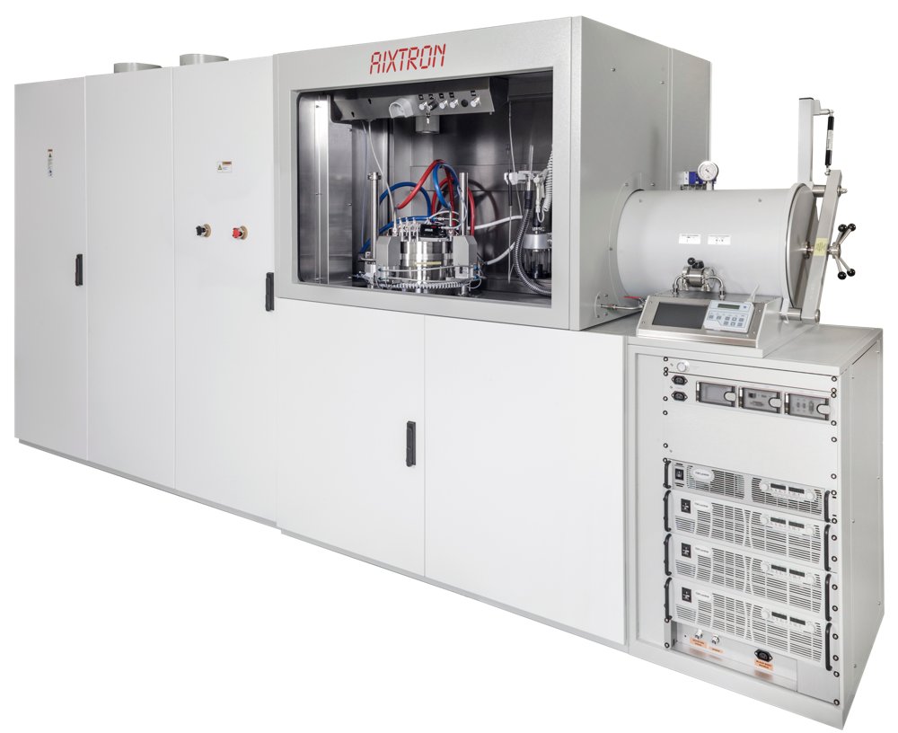
DEPOSITION SYSTEM FOR COMPOUND SEMICONDUCTORS “Flexible MOCVD system for R&D and small scale production” Key Benefits - Versatile R&D platform with integrated glovebox - True scaling from R&D to mass production - Inherently uniform and reproducible growth for all material systems - High flexibility in process window for excellent material quality and uniformity - Ideal for small R&D budgets: lowest running cost - Low gas flows and high precursor efficiency - Easy and low cost maintenance Product Features - High flexibility for various MO and hydride sources - Digital mass flow controllers and pressure controllers - Professional AIXACT® Advanced Control System with HTML-based GUI - Compact footprint CCS - Proven Close Coupled Showerhead® reactor with 3-zone heater - Dynamic process gap adjustment – effective process tuning for higher performance - 1400°C surface temperature option - In-situ monitoring with Laytec EpiTT, EpiCurveTT, and others on request - AIXTRON ARGUS full wafer temperature mapping - AIXTRON EPISON® gas concentration sensors Configurations (by simple carrier exchange): - 3x2 inch, 1x3 inch, 1x4 inch - 6x2 inch, 7x2 inch, 3x3 inch, 1x4 inch, 1x6 inch - 19x2 inch, 7x3 inch, 5x4 inch, 1x6 inch, 1x8 inch
CATEGORY
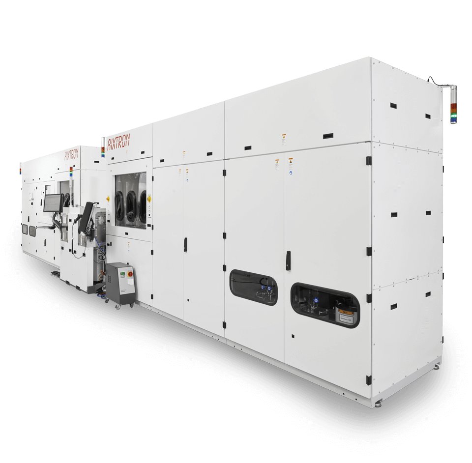
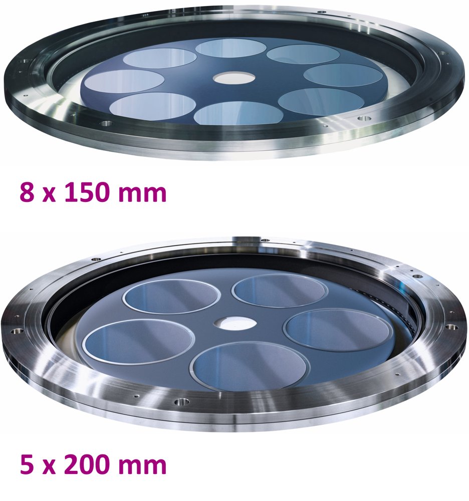
DEPOSITION SYSTEM FOR COMPOUND SEMICONDUCTORS “State-of-the-art Planetary reactor module for advanced GaN application on 150/200 mm substrates (Si/Sapphire/SiC) increases productivity and wafer performance” Key Benefits - Chosen by the best in the industry - Highest throughput - Lowest Cost of Ownership - Highest yield performance - 1st fully automated MOCVD platform with Cl2 in-situ cleaning and cassette-to-cassette wafer handler Product Features - Cost advantages of a batch reactor combined with the unique axis symmetric on-wafer uniformity of a single wafer reactor with respect to: wafer bow; layer thickness, material composition, dopant concentration; component yield - Warm ceiling provides lowest heat flux through the wafers: Minimized wafer curvature due to minimal vertical temperature gradients; Enables the use of Si wafers with standard thickness - Wafer temperature optimization through customer-specific design of the substrate pockets Configurations - 8x150 mm - 5x200 mm
CATEGORY
