By ASML
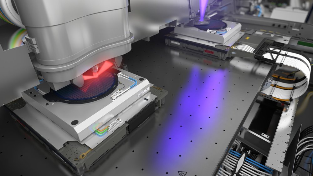
The PAS 5500/750F DUV Step-and-Scan system enables 130-nm mass production using mature 248-nm KrF technology. It combines the imaging power of the improved 0.7 NA 4x reduction lens with the latest multi-spot innovations in the leveling system and the AERIAL II illumination technology including QUASAR, multipole illumination and optional multiple exposure capability. The system is equipped with both TTL alignment and ATHENA for improved alignment accuracy on backend process layers, providing a long term single machine overlay of less than 25 nm. Further reduction of overhead times in combination with enhancements in productivity on customer jobs provide a production throughput of 130 200-mm wph. The application of a 2 kHz 20W KrF laser with Variable laser Frequency Control results in the lowest possible Cost of Operation. Technical Specifications Lens Wavelength: 248 nm NA: 0.5–0.7 (variable) Resolution: ≤ 130 nm Field size, for reticle with pellicle • Max X: 26.0 mm • Max Y: 33.0 mm CD Uniformity @ 0.13-μm L/SCD Uniformity @ 0.13-μm isolated lines • BF: ≤ 10 nm • Over 0.4-μm defocus: ≤ 15 nm CD Uniformity @ 0.13-μm isolated lines • BF: ≤ 10 nm • Over 0.4-μm defocus: ≤ 25 nm Distortion (Dynamic): ≤ 20 nm Overlay Single-machine: ≤ 25 nm Matched-machine: ≤ 40 nm AERIAL Illumination Annular • Intensity: ≥ 2400 mW/cm 2 (@ NA Max) • σ out: 0.35–0.88 • σ in: 0.10–0.58 • Integrated slit uniformity: ≤ 0.8% QUASAR ••• Production Throughput 50-mJ/cm 2 exposure dose • 200-mm wafers, 46 shots: ≥ 130 wph Lasers Type: Cymer ELS6600, Gigaphoton KES-G2OK Power: 20 W Frequency: Continuously variable up to 2 kHz Beam Delivery: ≤ 20-m remote capability Key Features and Benefits Variable, 0.7 NA Deep UV Projection Lens Production resolution down to 130 nm. Step and Scan Large field size, better CD control and lower lens aberrations. AERIAL II Illumination with QUASAR and Optional Multiple Exposure Capability Provides the ultimate flexibility in illumination modes at maximum throughput. PAS 5500 Step-and-Scan Body Commonality with i-line and 193-nm Step-and-Scan tools for economic mix-and-match. 8-Spot Level Sensor Improved focus and leveling under production conditions. ATHENA Advanced Alignment Increased alignment accuracy process latitude. Includes 2kHz 20W KrF Laser Technology with VariableLaser Frequency Control The perfect combination of high laser power for high throughput and efficient use of laser pulses for the lowest possible laser Cost of Operation.
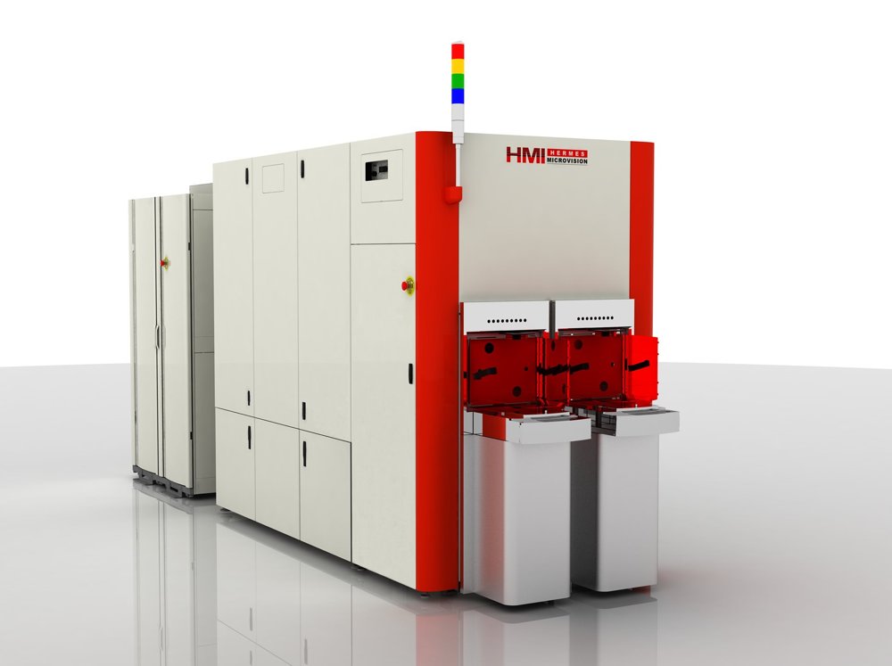
For today’s advanced microchips, defects as small as a couple of nanometers can render the entire chip useless. With its 1-nanometer resolution, e-beam inspection offers just the right kind of eyes to spot those tiny misprints. ASML is at the forefront of developments in e-beam metrology and inspection. E-beam achieves a higher resolution than YieldStar, but it measures more slowly, which means that it’s typically used after the pattern is etched onto the wafer. ‘E’ is for ‘electron’ E-beam technology has been around for decades. The basic concept is that a metal wire is heated until it gives off electrons, which are accelerated and formed into a beam by electric and magnetic fields. Unlike visible and ultraviolet light (but just like extreme ultraviolet light) electron beams must travel in a vacuum so they are not deflected or absorbed before reaching the target. In metrology and inspection in the semiconductor industry, the e-beam scans across the wafer. The electrons strike the surface and penetrate a small distance into the material, generating new 'secondary electrons' before being scattered. Just as with diffraction-based measurements, measuring the scattering of secondary electrons allows us to build up a very high-resolution picture of the surface. The more focused the beam, the smaller the details that can be measured. Speeding up e-beam imaging The tricky thing with e-beam measurements is that they’re quite slow. As a result, they have only typically been used in the early R&D phase of chip manufacturing, where time is less of an issue. ASML is leading the way in speeding up e-beam measurements so that manufacturers can enjoy their benefits in volume production. One way we do that is by developing solutions that focus e-beam measurements on specific hotspots where defects are more likely or more critical. In-line wafer and reticle inspection By speeding up the process and narrowing down the search to specific areas, e-beam can be used directly in the production line for wafer inspection while maintaining productivity levels.
CATEGORY
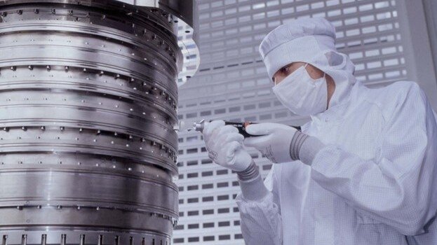
By autumn 2003, the immersion team was able to demonstrate concrete imaging results on the ASML prototype system dubbed the TWINSCAN AT:1150i. "The proto results changed the lithography roadmap almost instantly," Jan says. "We defined a series of new lithography systems in a very short period of time that would directly address the chip industry's resolution struggle."
CATEGORY
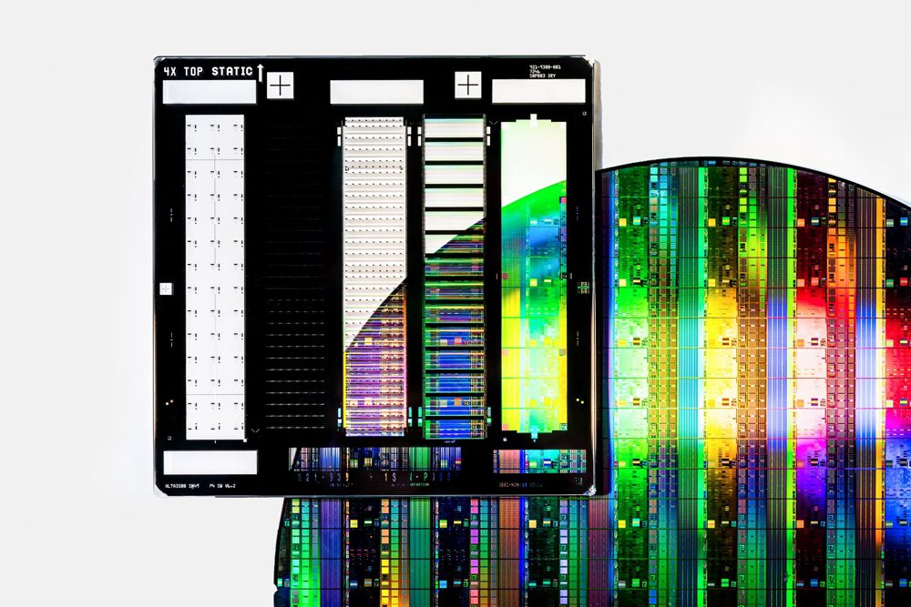
Using the vast amounts of data generated by our systems, computational lithography simulates the manufacturing process with powerful algorithms. These simulations help to design a chip blueprint (the reticle) that contains the pattern to be printed on the wafer. That's how we make sure that our lithography machines print what they should. This technique is called optical proximity correction (OPC) and is often combined with specific illumination optimizations in the lithography system. ASML's industry-leading computational lithography products enable accurate lithography simulations that help to improve chip yield and quality.
CATEGORY