We develop and produce the world’s first multi-beam mask writers for the global semiconductor industry. Nanotechnology at its best. We develop and produce electron-beam systems for the semiconductor industry. Our multi-beam mask writers are key tools for the production of integrated circuits.
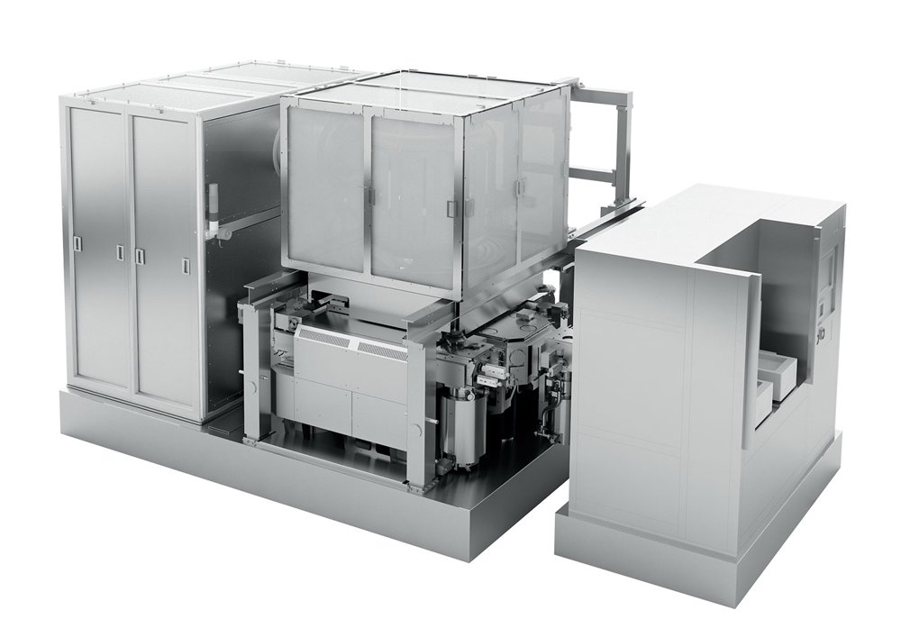
The first MBMW-201 2nd generation MBMW-201 tools for the 5-nanometer technology node will be delivered in 2019.
CATEGORY
The decisive advantage of our multi-beam mask writer over conventional technology (single variable shaped beam –V SB) is improved productivity, with a mask write time of less than 10 hours. This makes complex mask patterns possible, in particular for curvilinear Inverse Lithography Technology (ILT), without an increase in mask write times. TECHNICAL DATA - Electron beam energy at mask substrate: 50 keV - Programmable beams: 512 x 512 (262,144) - Multi-beam field: 82 µm x 82 µm - Resolution / positional accuracy: 14 nm / 0.1 nm - Maximum current density: 1 A/cm2 - Maximum electron current: 1 µA The fully-developed Multi-Beam Mask Writer (MBMW) offers both precision and exceptionally-high productivity for mask technology nodes from 28 to 5 nanometers (nm). As of 2016, IMS has been serving the mask industry with MBMW-101 mask writer production tools for use with the 7-nanometer technology node. The world’s first multi-beam mask writer for 6-inch photomasks, the MBMW Alpha tool, was realized in February 2014. In 2016, the MBMW’s data rate was increased by a factor of ten, to 120 Gbit/s. 1 Supply rack for high voltage, data path and system control 2 Electron-optical column 3 Platform with air-bearing vacuum stage 4 Automatic mask loading station
CATEGORY
