This silicon mold is primarily used in thermal nanoimprinting processes. Tekscend Photomask's silicon molds are manufactured by drawing a precise pattern on a photosensitive resist coated on a silicon substrate using an electron beam, and then deep drawing the pattern using a dry etching method. This process achieves the same high precision as quartz mold manufacturing and enables the production of silicon molds with high aspect ratio patterns and complex 3D shapes. Substrate size: 200 mm diameter (wafer thickness: 725 μm)
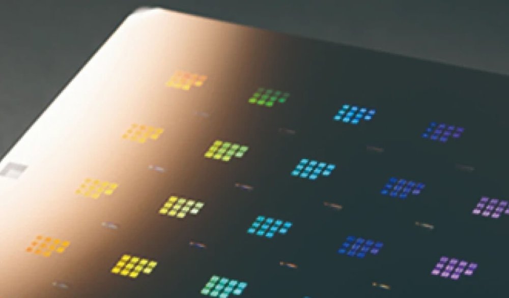
3D Mask (gray-scale mask, gray-tone mask) is a 3D photomask, applying the well-established photomask technology creating variable transmission of light across the photomask in order to facilitate creation of 3D structures. Microlens Structure (Prolith) Transferred Image of 3D mask (AFM image of resist profile) Examples of Pattern Types
CATEGORY
Tekscend Test pattern photomask form the basic-shaped pattern with chromium on the high purity glass substrate. Such photomasks are used for accuracy management of equipment, resolution checks, and evaluation of photoresist selection.
CATEGORY
This quartz mold is primarily used in the UV nanoimprint process. Tekscend Photomask's quartz molds are made of high-quality quartz substrate equivalent to that used for semiconductor photomasks, and have excellent stability and flatness. By applying the semiconductor photomask manufacturing process, our molds are capable of producing high-resolution patterns in the tens of nanometers. We also develop and manufacture molds with multi-step structures to meet a wide range of needs. Substrate size: 152 x 152 x 6.35 mm (t)
CATEGORY
