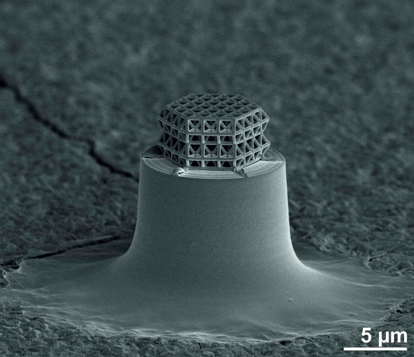
KIT scientists now present the smallest lattice structure made by man in the Nature Materials journal. Its struts and braces are made of glassy carbon and are less than 1 µm long and 200 nm in diameter. They are smaller than comparable metamaterials by a factor of 5. The small dimension results in so far unreached ratios of strength to density. Applications as electrodes, filters or optical components might be possible. (DOI: 10.1038/nmat4561)
"Lightweight construction materials, such as bones and wood, are found everywhere in nature," Dr.-Ing. Jens Bauer of Karlsruhe Institute of Technology (KIT), the first author of the study, explains. "They have a high load-bearing capacity and small weight and, hence, serve as models for mechanical metamaterials for technical applications."
Metamaterials are materials, whose structures of some micrometers (millionths of a meter) in dimension are planned and manufactured specifically for them to possess mechanical or optical properties that cannot be reached by unstructured solids. Examples are invisibility cloaks that guide light, sound or heat around objects, materials that counterintuitively react to pressure and shear (auxetic materials) or lightweight nanomaterials of high specific stability (force per unit area and density).
The smallest stable lattice structure worldwide presented now was produced by the established 3D laser lithography process at first. The desired structure of micrometer size is hardened in a photoresist by laser beams in a computer-controlled manner. However, resolution of this process is limited, such that struts of about 5 - 10 µm length and 1 µm in diameter can be produced only. In a subsequent step, the structure was therefore shrunk and vitrified by pyrolysis. For the first time, pyrolysis was used for manufacturing microstructured lattices. The object is exposed to temperatures of around 900°C in a vacuum furnace. As a result, chemical bonds reorient themselves. Except for carbon, all elements escape from the resist. The unordered carbon remains in the shrunk lattice structure in the form of glassy carbon. The resulting structures were tested for stability under pressure by the researchers.
"According to the results, load-bearing capacity of the lattice is very close to the theoretical limit and far above that of unstructured glassy carbon," Prof. Oliver Kraft, co-author of the study, reports. Until the end of last year, Kraft headed the Institute for Applied Materials of KIT. This year, he took over office as KIT Vice President for Research. "Diamond is the only solid having a higher specific stability."
Microstructured materials are often used for insulation or shock absorption. Open-pored materials may be used as filters in chemical industry. Metamaterials also have extraordinary optical properties that are applied in telecommunications. Glassy carbon is a high-technology material made of pure carbon. It combines glassy, ceramic properties with graphite properties and is of interest for use in electrodes of batteries or electrolysis systems.
KIT
#Bionano #MaterialScience
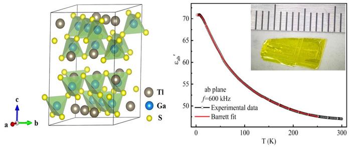
TlGaS2 single crystals show both in-plane and out-of-plane polarization, a rare combination in two-dimensional ferroelectrics that could widen options for ferroelectric transistors and non-volatile memory. Infrared spectroscopy revealed a soft phonon mode below 75 K, a signature tied to quantum ferroelectricity, along with weak structural changes across temperatures that lack clear heat-capacity signals, hinting at local rearrangements rather than conventional phase transitions.
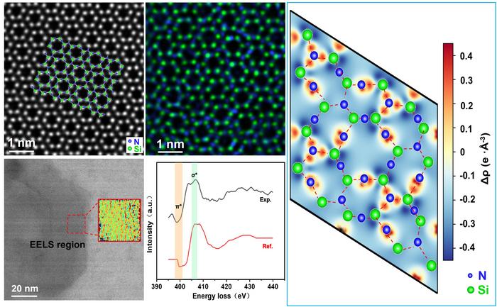
A β-Si3N4 nanolayer about 20 nm thick and continuous over several micrometers has been formed between carbon and silicon carbide without conventional oxide sintering additives, using a porous carbon framework infiltrated with molten silicon. Complementary atomic-resolution imaging resolved both silicon and nitrogen sublattices, confirming the ABAB stacking and corner-sharing tetrahedral network, while electron energy-loss spectroscopy and first-principles calculations linked the spectra to…
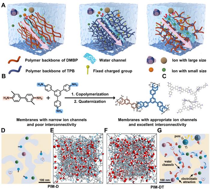
A polymer membrane with interconnected water-filled channels just 0.5 to 0.7 nanometers wide separates singly charged ions from multiply charged ones in both cationic and anionic systems. Built from Tröger's base-derived porous organic polymers, it cut the magnesium-to-lithium ratio in salt-lake brine roughly 500-fold across three electrodialysis stages, yielding 99.5 percent pure lithium carbonate, and enriched sodium chloride to 99.4 percent of ion mass from simulated seawater.
This week in nanotech
$740.7M raised
5 funding rounds · 36 deals tracked
New products
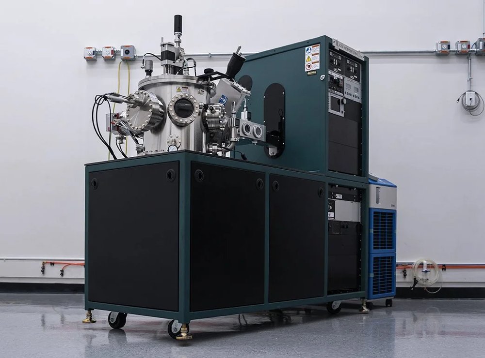 Orion Sputtering Deposition SystemsAJA International Featured
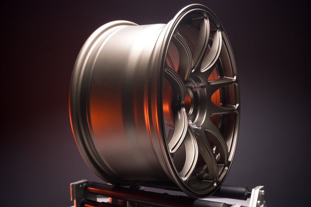 Ti-WCMBN Nanomaterialia Featured
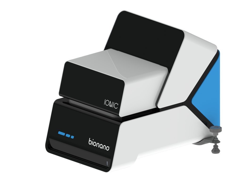 Ionic® Purification SystemBionano Genomics, Inc.
Market insights
Last 30 days: Quantum Technologies drew the most money: $3.18B.
Money raised per month