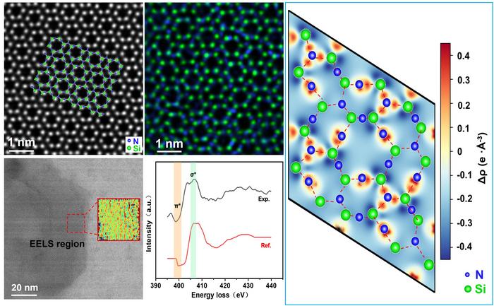
Silicon nitride combines high strength with thermal and chemical stability and electrical insulation, making it relevant to high-temperature structural components, thermal-management substrates and dielectric materials. These properties are closely connected to its atomic framework, in which silicon atoms are surrounded by four nitrogen atoms to form tetrahedra joined at their corners. Understanding this framework requires experimental observations that connect the positions of both elements with their local bonding and electronic states. Conventional silicon nitride ceramics usually rely on oxide additives to promote densification. After cooling, these additives can leave intergranular glassy phases or nanoscale boundary films and introduce local chemical variations. A continuous crystalline region formed without conventional sintering additives offers a useful setting for examining the silicon–nitrogen framework with fewer contributions from these additional chemical environments.
A team led by Xinghong Zhang at Harbin Institute of Technology and Suzhou Laboratory, China, has prepared such a region as a β-Si3N4 nanolayer between carbon and silicon carbide. The study, reported in Journal of Advanced Ceramics, combines reactive synthesis, complementary atomic-resolution imaging and bonding-sensitive spectroscopy. Yuhao Fang is the first author, and Wenzheng Zhang and Mingyi Tan are the corresponding authors.
The team published their work in Journal of Advanced Ceramics on October 16, 2026.
The researchers first prepared a hydrogel using glucose and nitrogen-containing components, then converted it into a porous carbon framework by vacuum pyrolysis at 1200 °C. Molten silicon infiltrated this framework at 1600 °C for 30 minutes. Silicon reacted with carbon to form silicon carbide, while nitrogen-containing species retained in the framework were proposed to supply nitrogen for the interfacial silicon nitride. No conventional oxide sintering additives were intentionally introduced during preparation. Microscopy revealed a distinct layer approximately 20 nm thick that extended continuously for more than 3 μm within the examined region. Elemental mapping located a narrow nitrogen-rich band between the neighboring carbon and silicon carbide regions. The combination of nanoscale thickness and micrometer-scale continuity provided a resolvable crystalline interior for targeted structural and spectroscopic analysis. To identify the crystal structure, the team combined high-angle annular dark-field scanning transmission electron microscopy with integrated differential phase-contrast imaging. The former resolved the projected silicon framework, while the latter also revealed the lighter nitrogen atomic columns. Observations along several crystallographic directions identified the characteristic ABAB stacking of β-Si3N4 and its corner-sharing tetrahedral network. This complementary approach allowed the silicon and nitrogen sublattices to be examined together within the same crystalline domain. Electron energy-loss spectroscopy then probed nitrogen- and silicon-specific features associated with unoccupied electronic states in that domain. The principal N K-edge and Si L2,3-edge features agreed with reference data and first-principles simulations, supporting their association with tetrahedral silicon-nitrogen coordination. A weak additional shoulder in the experimental nitrogen spectrum was tentatively linked to local lattice modulation or coordination perturbations, indicating how subtle structural variations can appear in the spectroscopic response. Electronic-structure calculations showed that occupied bonding states were weighted toward nitrogen, while unoccupied states had stronger silicon contributions and retained nitrogen character. Charge-density analysis indicated partial electron transfer from silicon to nitrogen together with directional electron sharing along the bonds, consistent with polar covalent bonding.
The work establishes a correspondence between atomic configuration and bonding-sensitive spectra within a continuous crystalline layer formed without conventional sintering additives. This experimental reference provides a basis for future comparisons of how additives, impurities, defects, strain and grain-boundary environments alter local silicon-nitrogen coordination and electronic states, helping clarify the atomic origins of property variations in silicon nitride and related covalent ceramics.
Reference
Formation and atomic-scale characterization of an interfacial β-Si3N4nanolayer in a C/SiC composite
Yuhao Fang, Wenzheng Zhang, Mingyi Tan, Daming Chen, Yanju Gu, Ao Chen, Chiyu Wang, Nan Qu, Lyu Yang, Xinghong Zhang, and Yanchun Zhou
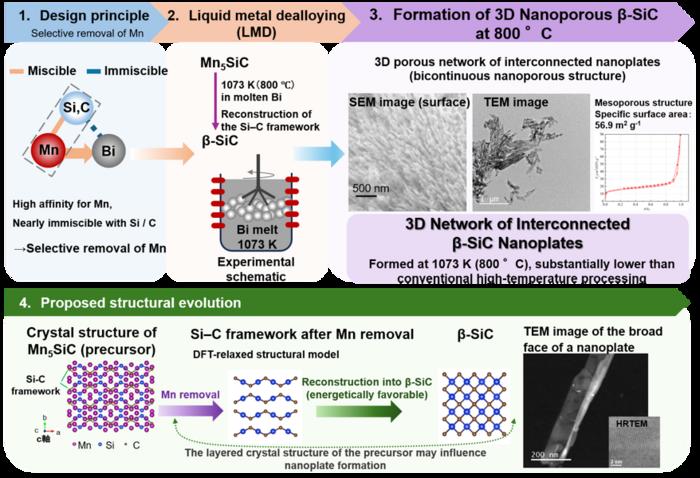
Researchers at Tohoku University have formed crystalline β-SiC at just 800°C using liquid metal dealloying, a technique previously limited to metals and intermetallics. Immersing a layered Mn5SiC precursor in molten bismuth selectively dissolves manganese, leaving a silicon-carbon framework that reorganizes into nanoporous β-SiC with interconnected nanoscale plates. First-principles calculations confirm the rearrangement is energetically favorable.
Wolfspeed has announced a multiyear supply agreement to provide silicon carbide devices for BorgWarner's next-generation 800V silicon carbide-based inverter platform. BorgWarner is using Wolfspeed's 1200V silicon carbide technology.
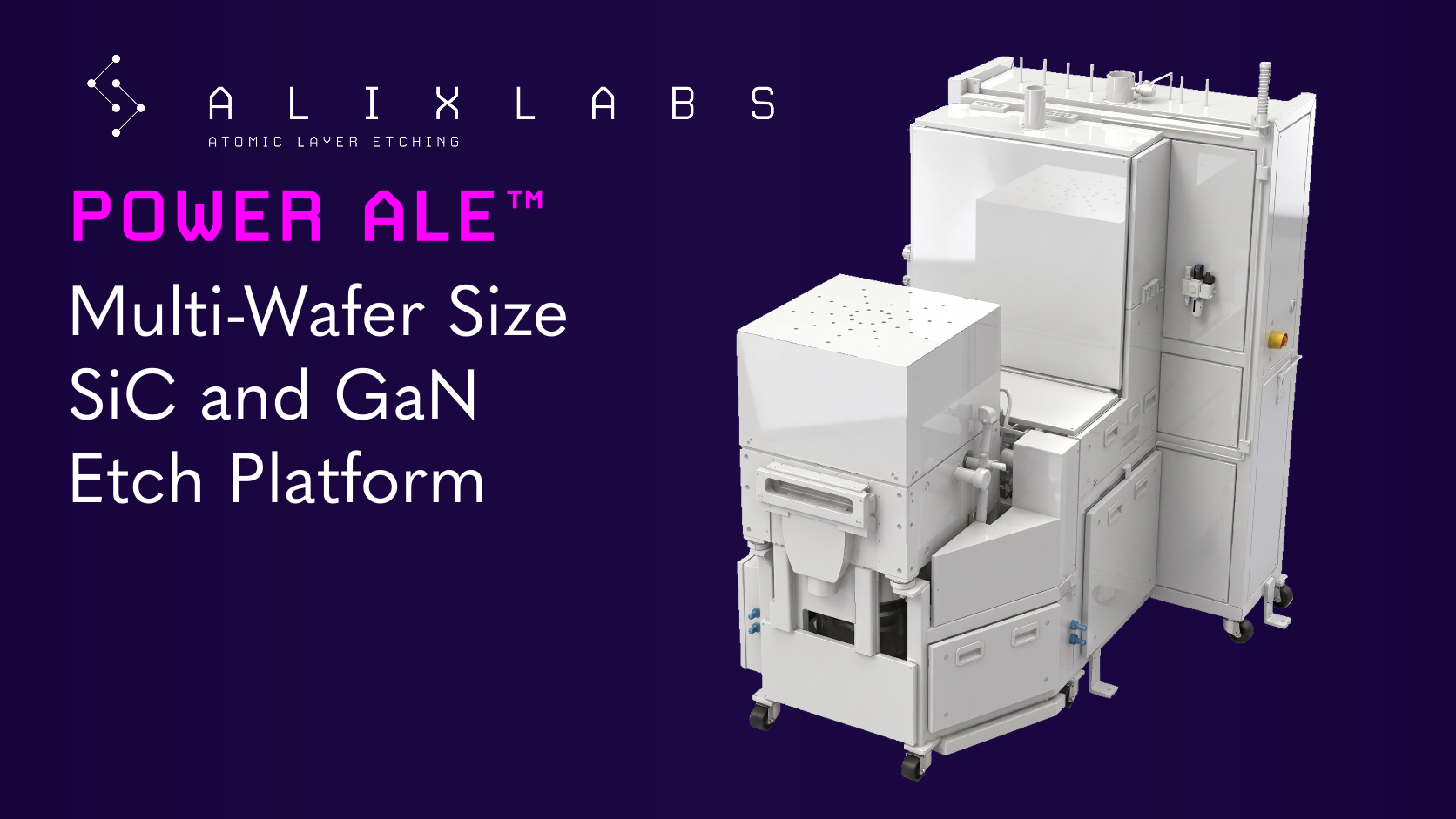
AlixLabs has introduced Power ALE™, an Atomic Layer Etching platform for wide-bandgap power semiconductors. It supports 150, 200 and 300 mm wafers and targets SiC trench sidewall smoothing and GaN HEMT gate recess.
This week in nanotech
$751.8M raised
6 funding rounds · 37 deals tracked
New products
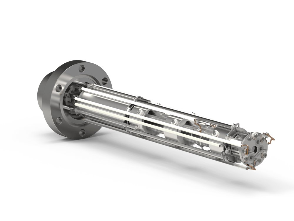 DLS-1 Mass Spectrometer for Fusion Gas AnalysisHiden Analytical Featured
 Nion-compatible In Situ STEM Holders for Electrical BiasingHummingbird Scientific Featured
 Hold Down & Release Mechanisms (HDRM) REACT – 5KN, 15KN and 35KN space qualified resettable mechanismsARQUIMEA
Market insights
Last 30 days: Quantum Technologies drew the most money: $3.18B.
Money raised per month