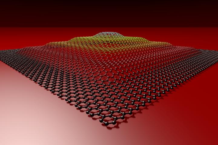
Researchers from Finland and Taiwan have discovered how graphene, a single-atom-thin layer of carbon, can be forged into three-dimensional objects by using laser light. A striking illustration was provided when the researchers fabricated a pyramid with a height of 60 nm, which is about 200 times larger than the thickness of a graphene sheet. The pyramid was so small that it would easily fit on a single strand of hair. The research was supported by the Academy of Finland and the Ministry of Science and Technology of the Republic of China.
Graphene is a close relative to graphite, which consists of millions of layers of graphene and can be found in common pencil tips. After graphene was first isolated in 2004, researchers have learned to routinely produce and handle it. Graphene can be used to make electronic and optoelectronic devices, such as transistors, photodetectors and sensors. In future, we will probably see an increasing number of products containing graphene.
"We call this technique optical forging, since the process resembles forging metals into 3D shapes with a hammer. In our case, a laser beam is the hammer that forges graphene into 3D shapes," explains Professor Mika Pettersson, who led the experimental team at the Nanoscience Center of the University of Jyväskylä, Finland. "The beauty of the technique is that it's fast and easy to use; it doesn't require any additional chemicals or processing. Despite the simplicity of the technique, we were very surprised initially when we observed that the laser beam induced such substantial changes on graphene. It took a while to understand what was happening."
"At first, we were flabbergasted. The experimental data simply made no sense," says Dr Pekka Koskinen, who was responsible for the theory. "But gradually, by close interplay between experiments and computer simulations, the actuality of 3D shapes and their formation mechanism started to become clear."
"When we first examined the irradiated graphene, we were expecting to find traces of chemical species incorporated into the graphene, but we couldn't find any. After some more careful inspections, we concluded that it must be purely structural defects, rather than chemical doping, that are responsible for such dramatic changes on graphene," explains Associate Professor Wei Yen Woon from Taiwan, who led the experimental group that carried out X-ray photoelectron spectroscopy at the synchrotron facility.
The novel 3D graphene is stable and it has electronic and optical properties that differ from normal 2D graphene. Optically forged graphene can help in fabricating 3D architectures for graphene-based devices.
The research was carried out at the Nanoscience Center (NSC) of the University of Jyväskylä, the National Central University of Taiwan and the National Synchrotron Radiation Research Center in Taiwan.
Andreas Johansson, Pasi Myllyperkiö, Pekka Koskinen, Jukka Aumanen, Juha Tapio Koivistoinen, Hung-Chieh Tsai, Chia-Hao Chen, Lo-Yueh Chang, Vesa-Matti Hiltunen, Jyrki Manninen, Wei-Yen Woon, and Mika Pettersson, Optical Forging of Graphene into Three-Dimensional Shapes. Nano Lett., DOI: 10.1021/acs.nanolett.7b03530
Academy of Finland
#Graphene

Waste polyamide-derived CQDs show continuous photoluminescence tuning from 308 to 552 nm through sequential defect-state engineering, with optical transition energies decreasing from 4.32 to 2.50 eV. @Christian Ebere Enyoh from Saitama University Carbon quantum dots (CQDs) are fluorescent carbon nanomaterials with potential applications in sensing, optoelectronics, displays, anti-counterfeiting, and environmental technologies. Their optical properties can be adjusted by modifying the carbon...

The researchers used circularly polarized light at normal incidence and found that helicity-dependent photocurrents appeared perpendicular to the crystal’s polarization but vanished when measured parallel to it, supporting a bulk origin of CPGE. @Institute of Science Tokyo The circular photogalvanic effect (CPGE), a phenomenon that generates helicity-dependent photocurrents in noncentrosymmetric materials, can originate purely from a crystal's internal structure without contribution from the...

Summary of gold nanoparticle growth programming in liposome based on localization of biomineralization peptide The position of biomineralization peptides within liposomes can influence how gold nanoparticles grow, reports a research team from Institute of Science Tokyo. Peptides localized at the membrane interface promote branched structures, while those confined to the liposome interior favor spherical nanoparticles. The findings offer a new strategy for controlling nanoscale reaction...
