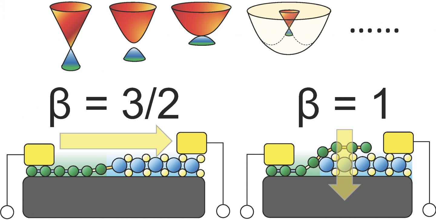
Schottky diode is composed of a metal in contact with a semiconductor. Despite its simple construction, Schottky diode is a tremendously useful component and is omnipresent in modern electronics. Schottky diode fabricated using two-dimensional (2D) materials have attracted major research spotlight in recent years due to their great promises in practical applications such as transistors, rectifiers, radio frequency generators, logic gates, solar cells, chemical sensors, photodetectors, flexible electronics and so on.
The understanding of 2D material-based Schottky diode is, however, plagued by multiple mysteries. Several theoretical models have co-existed in the literatures and a model is often selected a priori without rigorous justifications. It is not uncommon to see a model, whose underlying physics fundamentally contradicts with the physical properties of 2D materials, being deployed to analyse a 2D material Schottky diode.
Reporting in Physical Review Letters, researchers from the Singapore University of Technology and Design (SUTD) have made a major step forward in resolving the mysteries surrounding 2D material Schottky diode. By employing a rigorous theoretical analysis, they developed a new theory to describe different variants of 2D-material-based Schottky diodes under a unifying framework. The new theory lays down a foundation that helps to unite prior contrasting models, thus resolving a major confusion in 2D material electronics.
"A particularly remarkable finding is that the electrical current flowing across a 2D material Schottky diode follows a one-size-fits-all universal scaling law for many types of 2D materials," said first-author Dr. Yee Sin Ang from SUTD.
Universal scaling law is highly valuable in physics since it provides a practical "Swiss knife" for uncovering the inner workings of a physical system. Universal scaling law has appeared in many branches of physics, such as semiconductor, superconductor, fluid dynamics, mechanical fractures, and even in complex systems such as animal life span, election results, transportation and city growth.
The universal scaling law discovered by SUTD researchers dictates how electrical current varies with temperature and is widely applicable to broad classes of 2D systems including semiconductor quantum well, graphene, silicene, germanene, stanene, transition metal dichalcogenides and the thin-films of topological solids.
"The simple mathematical form of the scaling law is particularly useful for applied scientists and engineers in developing novel 2D material electronics," said co-author Prof. Hui Ying Yang from SUTD.
The scaling laws discovered by SUTD researchers provide a simple tool for the extraction of Schottky barrier height - a physical quantity critically important for performance optimisation of 2D material electronics.
"The new theory has far reaching impact in solid state physics," said co-author and principal investigator of this research, Prof. Lay Kee Ang from SUTD, "It signals the breakdown of classic diode equation widely used for traditional materials over the past 60 years, and shall improve our understanding on how to design better 2D material electronics."
Universal Scaling Laws in Schottky Heterostructures Based on Two-Dimensional Materials
Yee Sin Ang, Hui Ying Yang, and L. K. Ang
Phys. Rev. Lett. 121, 056802 – Published 1 August 2018
DOI: https://doi.org/10.1103/PhysRevLett.121.056802
Contact information:
Prof. Ang Lay Kee @ Ricky
SUTD Engineering Product Development
ricky_ang@sutd.edu.sg
Tel: +65 6499 4558
URL: http://people.sutd.edu.sg/ricky_ang/
Singapore University of Technology and Design (SUTD)
#2DMaterials #Nanoelectronics #Physics
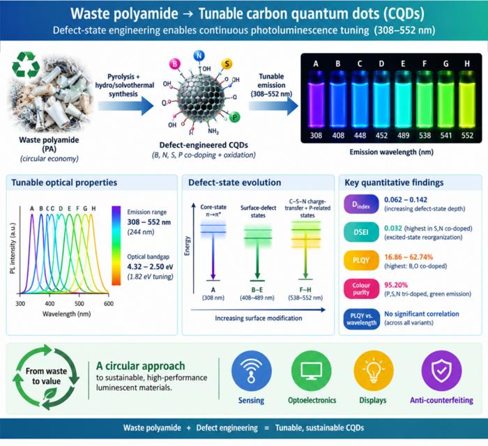
Waste polyamide-derived CQDs show continuous photoluminescence tuning from 308 to 552 nm through sequential defect-state engineering, with optical transition energies decreasing from 4.32 to 2.50 eV. @Christian Ebere Enyoh from Saitama University Carbon quantum dots (CQDs) are fluorescent carbon nanomaterials with potential applications in sensing, optoelectronics, displays, anti-counterfeiting, and environmental technologies. Their optical properties can be adjusted by modifying the carbon...
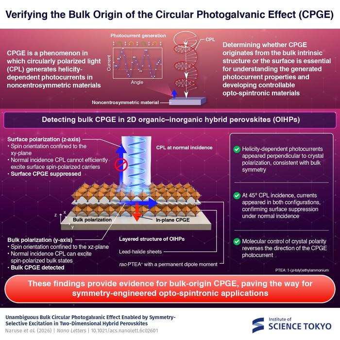
The researchers used circularly polarized light at normal incidence and found that helicity-dependent photocurrents appeared perpendicular to the crystal’s polarization but vanished when measured parallel to it, supporting a bulk origin of CPGE. @Institute of Science Tokyo The circular photogalvanic effect (CPGE), a phenomenon that generates helicity-dependent photocurrents in noncentrosymmetric materials, can originate purely from a crystal's internal structure without contribution from the...
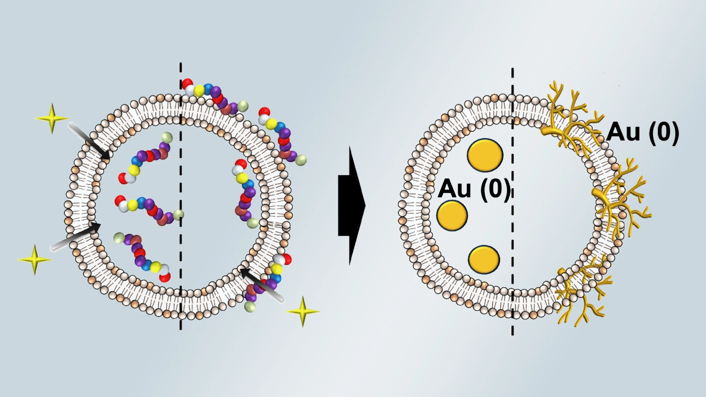
Summary of gold nanoparticle growth programming in liposome based on localization of biomineralization peptide The position of biomineralization peptides within liposomes can influence how gold nanoparticles grow, reports a research team from Institute of Science Tokyo. Peptides localized at the membrane interface promote branched structures, while those confined to the liposome interior favor spherical nanoparticles. The findings offer a new strategy for controlling nanoscale reaction...