Harvard John A. Paulson School of Engineering and Applied Sciences (SEAS)
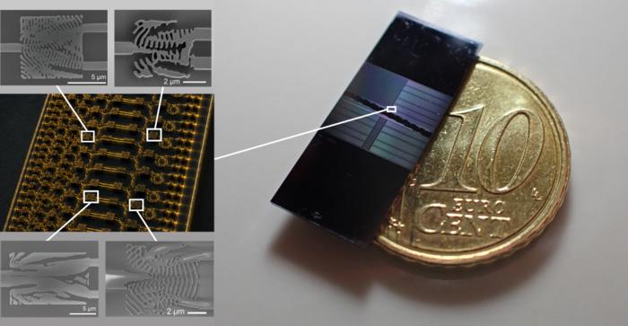
The extremely fast data-processing capabilities that power today’s telecommunications, large-scale AI data centers, quantum technologies and more, are enabled by photonic microchips – miniaturized semiconductors in which photons, rather than electrons, carry information through micrometer-wide waveguides.
Using a computer algorithm, researchers at the Harvard John A. Paulson School of Engineering and Applied Sciences (SEAS) and the Max Planck Institute for the Science of Light have developed three new functional components for photonic microchips that are each about 500 times smaller than conventional designs and offer a path toward higher-performance integrated light technologies. The results are published in Nature Communications.
Photonic microchips are made of many intricate parts, from grating couplers, which transfer light between fibers and waveguides, to ring resonators — tiny circular structures that temporarily store light and increase its intensity inside the chip. The design process for each component is time-consuming and tedious, with engineers typically starting with a familiar geometry and adjusting parameters as they go.
A research team co-led by Kiyoul Yang, SEAS assistant professor of electrical engineering, used a technique called inverse design to take an unconventional approach. Flipping the traditional process upside down, they first specified what they wanted the light to do. A computer algorithm then searched a large space of possible nanostructures for that exact function. The shapes the algorithm finds often look like irregular patterns of holes and ridges, but they nonetheless precisely guide light in a chip area that’s a tiny fraction the width of a human hair.
“Inverse design becomes practical when fabrication realities are built into the optimization,” said Yang, who co-led the work with Pascal Del’Haye, head of the microphotonics research group at Max Planck Institute. “By including minimum feature sizes and robustness to manufacturing variations in the algorithm itself, we obtain designs that are not only compact but also compatible with a commercial foundry process.”
Design and testing of devices
The team applied inverse design to silicon nitride – a material with low optical loss that can also help produce clean, laser-like light of many different colors. Previous approaches have mainly focused on silicon and, more recently, on diamond, silicon carbide and lithium niobate.
“Thick silicon nitride underpins most of the high-performance integrated photonics we work with, but until now its component library was limited to hand-engineered designs,” Del’Haye said. “These compact, computer-designed components are an important step towards more densely integrated nonlinear and quantum photonic circuits.”
The team designed, fabricated and tested three classes of device: wavelength splitters, which separate the colors of light; spatial mode sorters, which separate light into spatial channels; and mirrors.
As one of examples, inverse-designed mirrors, only a few micrometers across, reflect up to 98.5% of incoming light while blocking other spatial modes. Placed in pairs, they form on-chip optical cavities in which light bounces more than 100 times between the mirrors before escaping.
Future directions
The next step is to combine the newly developed components with nonlinear optical circuits. In these building blocks, intense light circulating on a chip can generate optical frequency combs: precise sets of many evenly spaced colors of light used in precision measurement, telecommunications and quantum technologies.
“Inverse design lets us define what we want light to do, and the optimization finds a structure that does it, often one no human would have drawn,” said Toby Bi, co-lead author of the study and researcher at the Max Planck Institute. “What is exciting is that the same framework can do three quite different jobs on the same chip: route light by wavelength, sort it by spatial mode, and act as compact mirrors that form on-chip optical cavities.”
“Inverse-designed silicon nitride nanophotonics” was co-authored by SEAS graduate students Egemen Bostan, and Danxian Liu, SEAS fellow and MIT EECS graduate student Aditya Paul, and postdoctoral fellow Tianyi Zeng.
The research was supported by the Defense Advanced Research Projects Agency (D23AP00251-00) and the Under Secretary of Defense for Research and Engineering (FA8721-05-C-0002). Device fabrication was carried out in part at the Harvard Center for Nanoscale Systems (National Science Foundation award No. 1541959).
Reference
Inverse-designed silicon nitride nanophotonics
Toby Bi, Shuangyou Zhang, Egemen Bostan, Danxian Liu, Aditya Paul, Olga Ohletz, Irina Harder, Yaojing Zhang, Alekhya Ghosh, Abdullah Alabbadi, Masoud Kheyri, Tianyi Zeng, Jesse Lu, Kiyoul Yang & Pascal Del’Haye
Nature Communications volume 17, Article number: 6943 (2026)

Wits and UEA researchers reveal a new free-space route to chiral light for sensing and photonics.
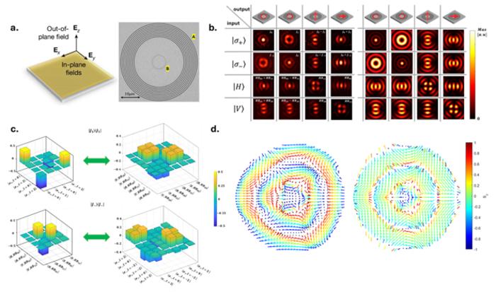
Technion researchers led by Prof. Guy Bartal have created the first on-chip nanophotonic platform that deterministically generates single-photon quantum skyrmions. Using a gold circular grating to control total angular momentum (TAM) of surface plasmons, the device transforms heralded single photons into robust, topologically protected SAM-OAM entangled states with skyrmion number ±2 — without post-selection or multi-photon entanglement. This breakthrough paves the way for scalable, high-dimensi
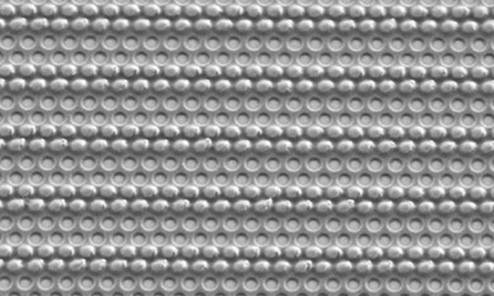
Most space missions rely on chemical rockets for propulsion. Rockets must carry fuel, which increases spacecraft mass and limits their speed and travel distance. For decades, researchers have explored light sails as an alternative. These devices use radiation pressure—the force exerted when light reflects from a surface—to generate thrust. When driven by a powerful laser, a light sail can accelerate continuously without onboard propellant, enabling faster travel across the solar system. Conve...
