Duiven, 27 October 2026. BE Semiconductor Industries N.V. acknowledged a press release from Applied Materials, Inc. in which Applied announced on October 26, 2026 an increase in its strategic share ownership to approximately 20% of Besi's outstanding shares.
According to Applied's release, Applied views its investment in Besi as long-term. Applied does not intend to seek board representation at Besi, nor does it currently have plans to purchase additional shares of Besi.
Besi and Applied have collaborated since 2020 on the development and commercialization of integrated hybrid bonding production systems for semiconductor manufacturers. The collaboration combines Applied's expertise in front-end manufacturing with Besi's technologies in die placement, interconnect and assembly solutions.
The companies have recently expanded their collaboration, with Besi joining Applied's EPIC Center as an Innovation Partner. Areas of collaboration target next-generation 3D IC scaling, logic and memory integration, the scaling of thermo-compression bonding and new die-on-wafer, die-on-die and die-on-panel integration platforms.
Richard W. Blickman, Besi's Chief Executive Officer, commented: "We welcome Applied's increased strategic investment as further confirmation of Besi's hybrid bonding and wafer-level assembly strategy. It also highlights future areas of potential collaboration between the companies targeting next generation AI and photonics systems for the industry's leading customers."
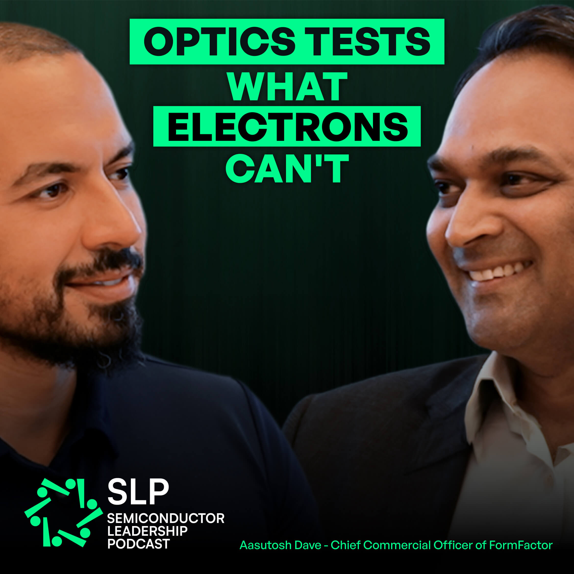
FormFactor CCO Aasutosh Dave discussed capacity constraints, silicon photonics test and the TRITON test cell on the Semiconductor Leadership Podcast episode published October 23, 2026.
Applied Materials opened its Equipment and Process Innovation and Commercialization (EPIC) Center in Silicon Valley on Oct. 12. The company bets $5 billion on the facility to develop future semiconductor technologies.
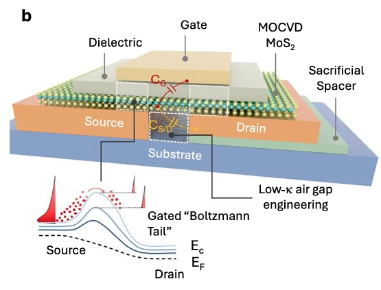
Researchers have fabricated transistors from molybdenum disulfide, an atomically thin two dimensional semiconductor, with channel lengths below five nanometers. An air gap beneath the channel lets the gate keep tighter control of current and curb leakage, delivering switching performance beyond silicon's theoretical limit at comparable size. The devices were built across a four inch wafer, pointing to manufacturability.
This week in nanotech
$282.2M raised
8 funding rounds · 36 deals tracked
New products
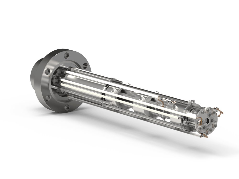 DLS-1 Mass Spectrometer for Fusion Gas AnalysisHiden Analytical Featured
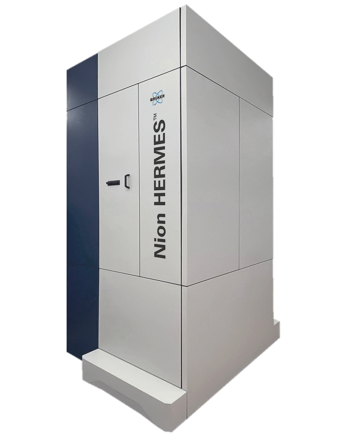 Nion-compatible In Situ STEM Holders for Electrical BiasingHummingbird Scientific Featured
 GiiiGii
Market insights
Last 30 days: Quantum Technologies drew the most money: $3.17B.
Money raised per month
Behind the deal
Who invested in Vertical Semiconductor’s $73M Grant?
See the investors with Insights Pro →