World Scientific
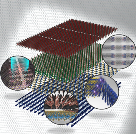
In a paper published in NANO, a group of researchers from Sungkyunkwan University, South Korea provide a comprehensive review of heterogeneously integrated two dimensional (2D) materials from an extensive library of atomic 2D materials with selectable material properties to open up fascinating possibilities for the design of functional novel devices.
Since the discovery of Graphene by Andre Geim and Konstantin Novoselov, 2D materials, e.g., graphene, black phosphorous (BP), transition metal dichalcogenides (TMDCs), and hexagonal boron nitride (h-BN) have attracted extensive attention due to their broad physical properties and wide range of applications to electronic and optoelectronic devices. Research on these 2D materials has matured to the point where an extensive library of atomically thin 2D materials with selectable material properties has been created and continues to grow.
By combining or stacking these 2D materials, it is possible to construct 2D heterostructures, which are built by directly stacking individual monolayers comprising different materials. Each monolayer within a 2D heterostructure is highly stable, due to strong covalent bonds between the atoms within that monolayer. However, the forces between the monolayers that keep said monolayers stacked one above the other to form the 2D heterostructure happen to be relatively weak van der Waals interactions. Due to this, each of the monolayers retains its intrinsic properties. Moreover, unlike in conventional semiconductor heterostructures where component material selection is restricted to those with similar lattice structures, the lattice mismatch requirements of stacked heterostructures can be relaxed due to the weakness of the van der Waal's forces. This means that one can combine insulating, semiconducting, or metallic 2D materials to form a single 2D heterostructure despite their different lattice structures.
When a monolayer is stacked in combination with other monolayers made out of different materials, a variety of new heterostructures with atomically thin 2D heterojunctions can be created. Heterostructures made from a particular combination of materials will have a certain set of physical characteristics depending on which materials they are made from. The unusual physical characteristics of 2D heterostructures make them suitable for use in a wide range of applications.
In this review, various 2D heterostructures are discussed along with an explanation of novel electronic and optoelectronic properties, advanced synthesis technical developments, as well as new functional applications available. It provides an understanding of the current research trends in 2D materials, so as to explore future possibilities for nanomaterial research.
Heterogeneous Integration of 2D Materials: Recent Advances in Fabrication and Functional Device Applications
Indhana Veera Sankar, Jaeho Jeon, Sung Kyu Jang, Jeong Ho Cho, Euyheon Hwang and Sungjoo Lee
Nano Vol. 14, No. 12, 1930009 (2019)
DOI: 10.1142/S1793292019300093
Contact information:
Associate Professor at SKKU Advanced Institute of Nanotechnology (SAINT)
euyheon@skku.edu
Phone: +82-31-299-4163
Professor at SKKU Advanced Institute of Nanotechnology (SAINT)
leesj@skku.edu
Phone: +82-31-299-4169
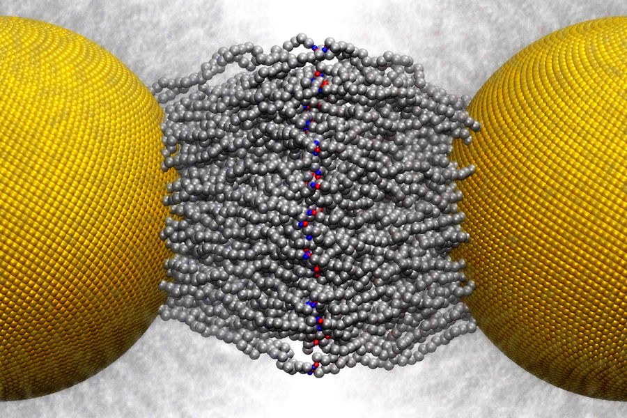
Researchers have shown that super-flexible connector molecules, rather than rigid ones, can tune how nanoparticles pack into larger structures. By varying ligand chain length, particle size and electric charge, the team assembled nanoparticles into crystal lattices never seen before and controlled the number of bonds each particle forms.
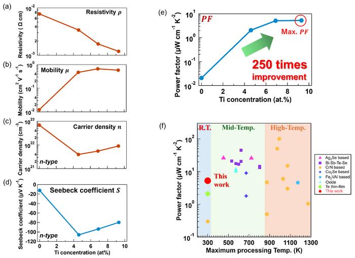
Researchers at Tohoku University have raised the power factor of chromium nitride thin films 250-fold by doping them with small amounts of titanium, reaching 5.26 µW cm⁻¹ K⁻². Titanium's stronger affinity for nitrogen suppresses nitrogen vacancies, cutting carrier concentration while boosting electron mobility by roughly two orders of magnitude.
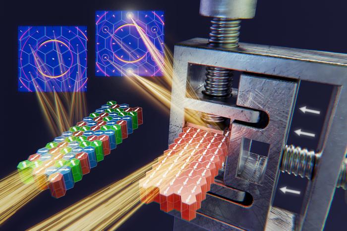
Neutron diffraction at Oak Ridge National Laboratory has shown that a modest mechanical squeeze can substantially reshape the magnetic behavior of altermagnets, a class of materials under investigation for spintronics. Squeezing manganese telluride and iron sulfide crystals between titanium plates altered their magnetic domain populations and changed the anomalous Hall effect, which governs electron transport.
This week in nanotech
$3.4M raised
1 funding round · 17 deals tracked
New products
 Nion-compatible In Situ STEM Holders for Electrical BiasingHummingbird Scientific Featured
 Ti-WCMBN Nanomaterialia Featured
 Hold Down & Release Mechanisms (HDRM) REACT – 5KN, 15KN and 35KN space qualified resettable mechanismsARQUIMEA
Market insights
Last 30 days: Quantum Technologies was the busiest vertical: 60 of 192 events (31%).
Money raised per month
Behind the deal
Who led Sandia National Laboratories’s $3.4M Grant?
See the investors with Insights Pro →