Ludwig Maximilian University of Munich
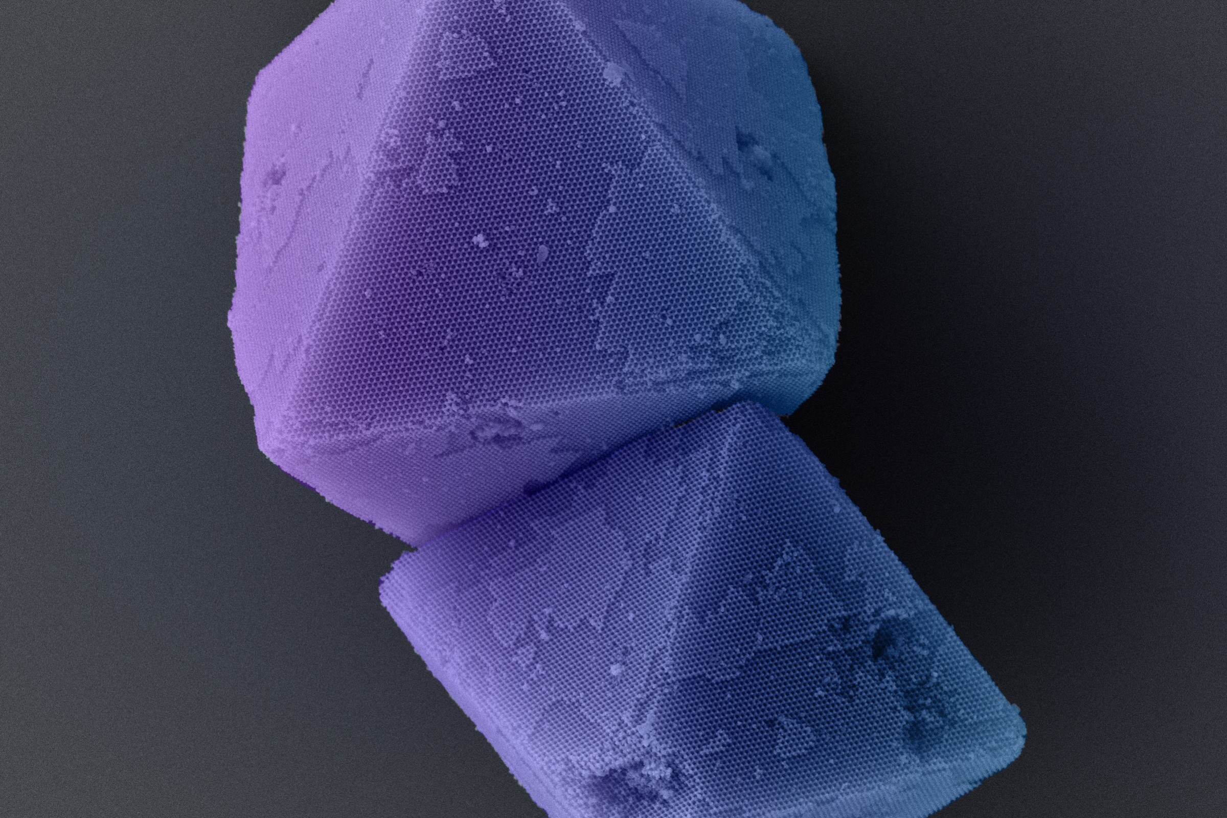
The shimmering of butterfly wings in bright colors does not emerge from pigments. Rather, it is photonic crystals that are responsible for the play of colors. Their periodic nanostructure allows light at certain wavelengths to pass through while reflecting other wavelengths. This causes the wing scales, which are in fact transparent, to appear so magnificently colored. For research teams, the manufacture of artificial photonic crystals for visible light wavelengths has been a major challenge and motivation ever since they were predicted by theorists more than 35 years ago. “Photonic crystals have a versatile range of applications. They have been employed to develop more efficient solar cells, innovative optical waveguides, and materials for quantum communication. However, they have been very laborious to manufacture,” explains Dr. Gregor Posnjak. The physicist is a postdoc in the research group of LMU Professor Tim Liedl, whose work is funded by the “e-conversion” Cluster of Excellence and the European Research Council. Using DNA nanotechnology, the team has developed a new approach for the manufacture of photonic crystals. Their results have now been published in the journal Science.
Diamond structure out of strands of DNA
In contrast to lithographic techniques, the LMU team uses a method called DNA origami to design and synthesize building blocks, which then self-assemble into a specific lattice structure. “It’s long been known that the diamond lattice theoretically has an optimal geometry for photonic crystals. In diamonds, each carbon atom is bonded to four other carbon atoms. Our challenge consisted in enlarging the structure of a diamond crystal by a factor of 500, so that the spaces between the building blocks correspond with the wavelength of light,” explains Tim Liedl. “We increased the periodicity of the lattice to 170 nanometers by replacing the individual atoms with larger building blocks – in our case, through DNA origami,” says Posnjak.
The perfect molecule folding technique
What sounds like magic is actually a specialty of the Liedl group, one of the world’s leading research teams in DNA origami and self-assembly. For this purpose, the scientists use a long, ring-shaped DNA strand (consisting of around 8,000 bases) and a set of 200 short DNA staples. “The latter control the folding of the longer DNA strand into virtually any shape at all – akin to origami masters, who fold pieces of paper into intricate objects. As such, the clamps are a means of determining how the DNA origami objects combine to form the desired diamond lattice,” says the LMU postdoctoral researcher. The DNA origami building blocks form crystals of approximately ten micrometers in size, which are deposited on a substrate and then passed on to a cooperating research group from the Walter Schottky Institute at the Technical University of Munich (TUM): The team led by Professor Ian Sharp (also funded by the “e-conversion” Cluster of Excellence) is able to deposit individual atomic layers of titanium dioxide on all surfaces of the DNA origami crystals. “The DNA origami diamond lattice serves as scaffolding for titanium dioxide, which, on account of its high index of refraction, determines the photonic properties of the lattice. After coating, our photonic crystal does not allow UV light with a wavelength of about 300 nanometers to pass through, but rather reflects it,” explains Posnjak. The wavelength of the reflected light can be controlled via the thickness of the titanium dioxide layer.
DNA origami could boost photonics
For photonic crystals that work in the infrared range, classic lithographic techniques are suitable but laborious and expensive. In the wavelength range of visible and UV light, lithographic methods have not been successful to date. “Consequently, the comparatively easy manufacturing process using the self-assembly of DNA origami in an aqueous solution offers a powerful alternative for producing structures in the desired size cost-effectively and in larger quantities,” says Prof. Tim Liedl. He is convinced that the unique structure with its large pores, which are chemically addressable, will stimulate further research – for example, in the domain of energy harvesting and storage. In the same issue of Science, a collaboration led by prof. Petr Šulc of Arizona State University and TUM presents a theoretical framework for designing diverse crystalline lattices from patchy colloids, and experimentally demonstrates the method by utilizing DNA origami building blocks to form a pyrochlore lattice, which potentially also could be used for photonic applications.
Reference
Diamond-lattice photonic crystals assembled from DNA origami
Gregor Posnjak, Xin Yin, Paul Butler, Oliver Bienek, Mihir Dass, Seungwoo Lee, Ian D. Sharp, Tim Liedl
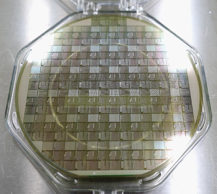
A junction transistor fabricated on a 6-inch SiC epi-wafer. Kyoto, Japan -- While silicon carbide -- SiC -- has long been promoted as the key to developing electronics suitable for extreme environments, the field has been stuck in the lab for some time. Now, a team of researchers focusing on junction field-effect transistors, or JFETs, have succeeded in developing a new SiC transistor structure that can operate at 600°C, as announced recently by Kyoto University.* One of the team's goals...
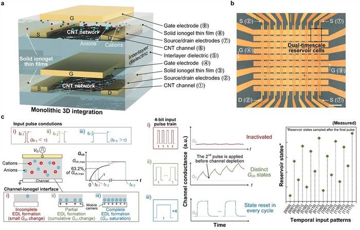
Figure 1. Monolithic 3D-integrated multi-timescale reservoir architecture based on solid ion-gated transistors Thin-film carbon nanotube (CNT) ion-gated transistors were fabricated using an ionogel, in which ions are embedded in a polymer matrix to form a solid. By varying the ionic content, the transistors were designed to show different ionic dynamics and response times. Devices with different time characteristics were then stacked vertically to create a 3D reservoir architecture that can...

Autferroic nanomaterials protect everyday data while bringing quantumlike computing to standard microchips Behind every secure online transaction or encrypted message lies a string of completely unpredictable numbers. A team of physicists has now theoretically eliminated a long-standing roadblock, opening the door for next-generation security chips that protect everyday data without slowing down performance. In a study published in “Physical Review Letters,” a research team co-led by Rice...
