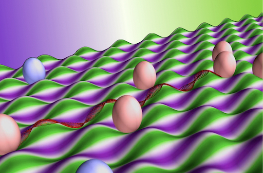
Lay some graphene down on a wavy surface, and you’ll get a guide to one possible future of two-dimensional electronics.
Rice University scientists put forth the idea that growing atom-thick graphene on a gently textured surface creates peaks and valleys in the sheets that turn them into “pseudo-electromagnetic” devices.
The channels create their own minute but detectable magnetic fields. According to a study by materials theorist Boris Yakobson, alumnus Henry Yu and research scientist Alex Kutana at Rice’s George R. Brown School of Engineering, these could facilitate nanoscale optical devices like converging lenses or collimators.
Their study appears in the American Chemical Society’s Nano Letters.
They also promise a way to achieve a Hall effect — a voltage difference across the strongly conducting graphene — that could facilitate valleytronics applications that manipulate how electrons are trapped in “valleys” in an electronic band structure.
Valleytronics are related to spintronics, in which a device’s memory bits are defined by an electron’s quantum spin state. But in valleytronics, electrons have degrees of freedom in the multiple momentum states (or valleys) they occupy. These can also be read as bits.
This is all possible because graphene, while it may be one of the strongest known structures, is pliable enough as it adheres to a surface during chemical vapor deposition.
“Substrate sculpting imparts deformation, which in turn alters the material electronic structure and changes its optical response or electric conductivity,” said Yu, now a postdoctoral researcher at Lawrence Livermore National Laboratory. “For sharper substrate features beyond the pliability of the material, one can engineer defect placements in the materials, which creates even more drastic changes in material properties.”
Yakobson compared the process to depositing a sheet of graphene on an egg crate. The bumps in the crate deform the graphene, stressing it in a way that creates an electromagnetic field even without electrical or magnetic input.
“The endless designs of substrate shapes allow for countless optical devices that can be created, making possible 2D electron optics,” Yakobson said. “This technology is a precise and efficient way of transmitting material carriers in 2D electronic devices, compared to traditional methods.”
Reference
Electron Optics and Valley Hall Effect of Undulated Graphene
Henry Yu, Alex Kutana, and Boris I. Yakobson

Waste polyamide-derived CQDs show continuous photoluminescence tuning from 308 to 552 nm through sequential defect-state engineering, with optical transition energies decreasing from 4.32 to 2.50 eV. @Christian Ebere Enyoh from Saitama University Carbon quantum dots (CQDs) are fluorescent carbon nanomaterials with potential applications in sensing, optoelectronics, displays, anti-counterfeiting, and environmental technologies. Their optical properties can be adjusted by modifying the carbon...

The researchers used circularly polarized light at normal incidence and found that helicity-dependent photocurrents appeared perpendicular to the crystal’s polarization but vanished when measured parallel to it, supporting a bulk origin of CPGE. @Institute of Science Tokyo The circular photogalvanic effect (CPGE), a phenomenon that generates helicity-dependent photocurrents in noncentrosymmetric materials, can originate purely from a crystal's internal structure without contribution from the...

Summary of gold nanoparticle growth programming in liposome based on localization of biomineralization peptide The position of biomineralization peptides within liposomes can influence how gold nanoparticles grow, reports a research team from Institute of Science Tokyo. Peptides localized at the membrane interface promote branched structures, while those confined to the liposome interior favor spherical nanoparticles. The findings offer a new strategy for controlling nanoscale reaction...
