University of Oxford
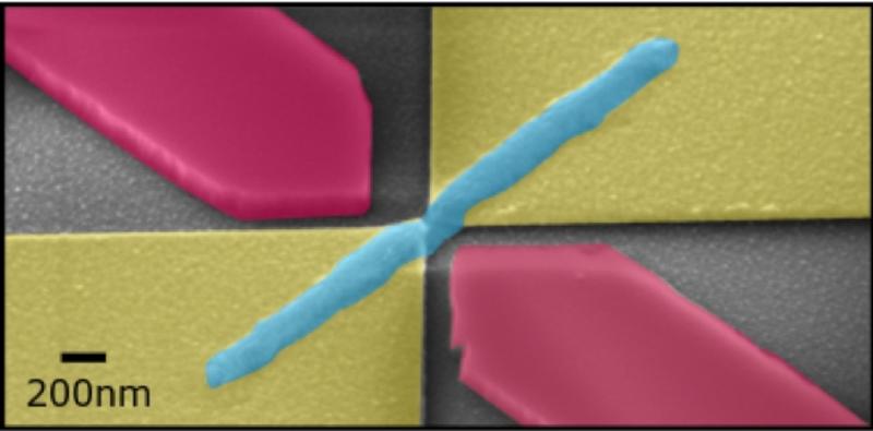
In collaboration with researchers at the universities of Münster and Exeter, scientists have created a first-of-a-kind electro-optical device which bridges the fields of optical and electronic computing. This provides an elegant solution to achieving faster and more energy efficient memories and processors.
Computing at the speed of light has been an enticing but elusive prospect, but with this development it's now in tangible proximity. Using light to encode as well as transfer information enables these processes to occur at the ultimate speed limit - that of light. While as of recently, using light for certain processes has been experimentally demonstrated, a compact device to interface with the electronic architecture of traditional computers has been lacking. The incompatibility of electrical and light-based computing fundamentally stems from the different interaction volumes that electrons and photons operate in. Electrical chips need to be small to operate efficiently, whereas optical chips need to be large, as the wavelength of light is larger than that of electrons.
To overcome this challenging problem the scientists came up with a solution to confine light into nanoscopic dimensions, as detailed in their paper Plasmonic nanogap enhanced phase change devices with dual electrical-optical functionality published in Science Advances, 29 November 2019. They created a design which allowed them to compress light into a nano-sized volume through what is known as surface plasmon polariton. The dramatic size reduction in conjunction with the significantly increased energy density is what has allowed them to bridge the apparent incompatibility of photons and electrons for data storage and computation. More specifically, it was shown that by sending either electrical or optical signals, the state of a photo- and electro-sensitive material was transformed between two different states of molecular order. Further, the state of this phase-transforming material was read out by either light or electronics thereby making the device the first electro-optical nanoscale memory cell with non-volatile characteristics.
"This is a very promising path forward in computation and especially in fields where high processing efficiency is needed," states Nikolaos Farmakidis, graduate student and co-first author.
Co-author Nathan Youngblood continues: "This naturally includes artificial intelligence applications where in many occasions the needs for high-performance, low-power computing far exceeds our current capabilities. It is believed that interfacing light-based photonic computing with its electrical counterpart is the key to the next chapter in CMOS technologies."
Plasmonic nanogap enhanced phase-change devices with dual electrical-optical functionality
Nikolaos Farmakidis, Nathan Youngblood, Xuan Li, James Tan, Jacob L. Swett, Zengguang Cheng, C. David Wright, Wolfram H. P. Pernice and Harish Bhaskaran
Science Advances (2019) Vol. 5, no. 11, eaaw2687
Contact information:
Harish Bhaskaran
Oxford Professor of Applied Nanomaterials
harish.bhaskaran@materials.ox.ac.uk
Phone: +44-1865-273772
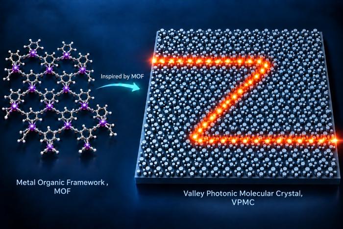
Inspired by Metal-Organic Framework based topological insulators, researchers at Tsinghua University proposed valley photonic molecular crystal (VPMC) and investigated the impact of molecular rotation on the valley-topological properties of VPMC. Credit: Tsinghua University/Xue Feng A research team led by Yidong Huang at Tsinghua University, including Xue Feng and Yongzhuo Li, has developed valley photonic molecular crystals (VPMCs) on a silicon platform. Combining theoretical modeling,...
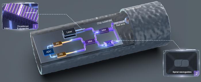
The system integrates a III-V semiconductor light source, SiN-based interferometers, Si-Ge photodetectors (PDs), and an integrated ball-lens microprobe, thereby combining the distinct advantages of multiple photonic integration platforms. The insets illustrate complementary technologies that can be incorporated to realize a miniaturized, fully integrated OCT system. Abbreviations: ADC, analog-to-digital converter. Inset 1: Foundry-scalable embedded III-V lasers on silicon-on-insulator (SOI)...

From left to right: Three photons with different quantum states enter an interferometer with three beam splitters. At each beam splitter, they can take different paths at the same time in superposition. The researchers then measured how often the three photons ended up together at the same output. Counterintuitively, it is possible to make the photons more similar to each other and at the same make them less likely to “bunch” together. AI-generated illustration, by Leonardo Novo. We usually...
