top of page
NEWSROOM


Toward practical laser-driven light sails using photonic crystals
Most space missions rely on chemical rockets for propulsion. Rockets must carry fuel, which increases spacecraft mass and limits their speed and travel distance. For decades, researchers have explored light sails as an alternative. These devices use radiation pressure—the force exerted when light reflects from a surface—to generate thrust. When driven by a powerful laser, a light sail can accelerate continuously without onboard propellant, enabling faster travel across the so
Mar 113 min read


Realization of the Tellegen effect in resonant optical metasurfaces
Nonreciprocal interactions between light and matter lie at the heart of many exotic physical phenomena, from magnet-free optical isolation to axion-inspired electrodynamics. One particularly intriguing example is the Tellegen effect, a nonreciprocal magnetoelectric coupling predicted more than 75 years ago but long considered weak and negligible at optical frequencies. “In natural materials, the optical Tellegen effect is extraordinarily weak, making it challenging to observe
Mar 32 min read


Researchers build ultra-efficient optical sensors shrinking light to a chip
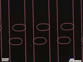
Optical waveguide microresonators on a chip created in this effort, which are ten times thinner than human hair. @CU Boulder College of Engineering and Applied Science CU Boulder researchers have built high performing optical microresonators opening the door for new sensor technologies. At its simplest form, a microresonator is a tiny device that can trap light and build up its intensity. Once the intensity is high enough, researchers can perform unique light operations. “O
Feb 244 min read


Focusing and Defocusing Light Without a Lens
Illustration of the spatially structured self-imaging phenomenon known as the Montgomery effect. The color palette corresponds to the phase profile of the light, revealing the helical wavefront of light with orbital angular momentum, re-appearing over propagation. @ Joshua Mornhinweg First demonstration of the structured Montgomery effect in free space Applied physicists in the Harvard John A. Paulson School of Engineering and Applied Sciences (SEAS) have demonstrated a new w
Feb 93 min read


An unexpected breakthrough in flat optics
An unexpected discovery in a Harvard lab has led to a breakthrough insight into choosing an unconventional material, silica, to make optical metasurfaces – ultra-thin, flat structures that control light at the nanoscale and are already replacing traditional optical devices like lenses and mirrors. A team from Harvard's John A. Paulson School of Engineering and Applied Sciences and collaborators at the University of Lisbon has found that in some cases, silica — the fundamental
Jan 154 min read


Scientists create stable, switchable vortex knots inside liquid crystals
In a new Nature Physics study, researchers created particle-like so-called “vortex knots” inside chiral nematic liquid crystals, a twisted fluid similar to those used in LCD screens. For the first time, these knots are stable and could be reversibly switched between different knotted forms, using electric pulses to fuse and split them.
Dec 17, 20255 min read
bottom of page