Miniaturisation ranks as the driving force behind the semiconductor industry. The tremendous gains in computer performance since the 1950s are largely due to the fact that ever smaller structures can be manufactured on silicon chips. Chemical engineers at ETH Zurich have now succeeded in reducing the size of organic light-emitting diodes (OLEDs) - which are currently primarily in use in premium mobile phones and TV screens - by several orders of magnitude. Their study was recently published in the journal Nature Photonics.
Miniaturised in one single step
Light-emitting diodes are electronic chips made of semiconductor materials that convert electrical current into light. "The diameter of the most minute OLED pixels we have developed to date is in the range of 100 nanometres, which means they are around 50 times smaller than the current state of the art," explains Jiwoo Oh, a doctoral student active in the nanomaterial engineering research group headed by ETH Professor Chih-Jen Shih.
Oh developed the process for manufacturing the new nano-OLEDs together with Tommaso Marcato. "In just one single step, the maximum pixel density is now around 2500 times greater than before," adds Marcato, who is active as a postdoc in Shih's group.
By way of comparison: up to the 2000s, the miniaturisation pace of computer processors followed Moore's Law, according to which the density of electronic elements doubled every two years.
Screens, microscopes and sensors
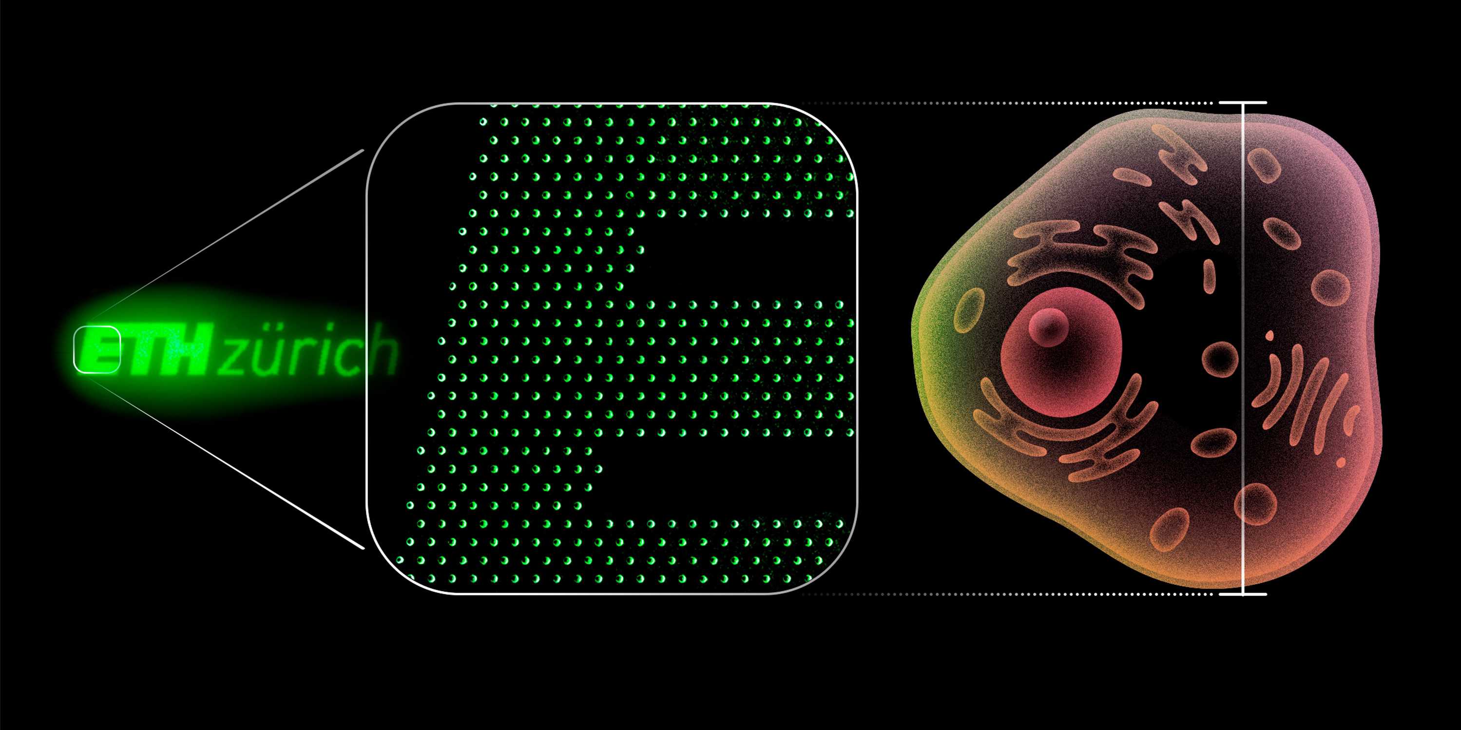
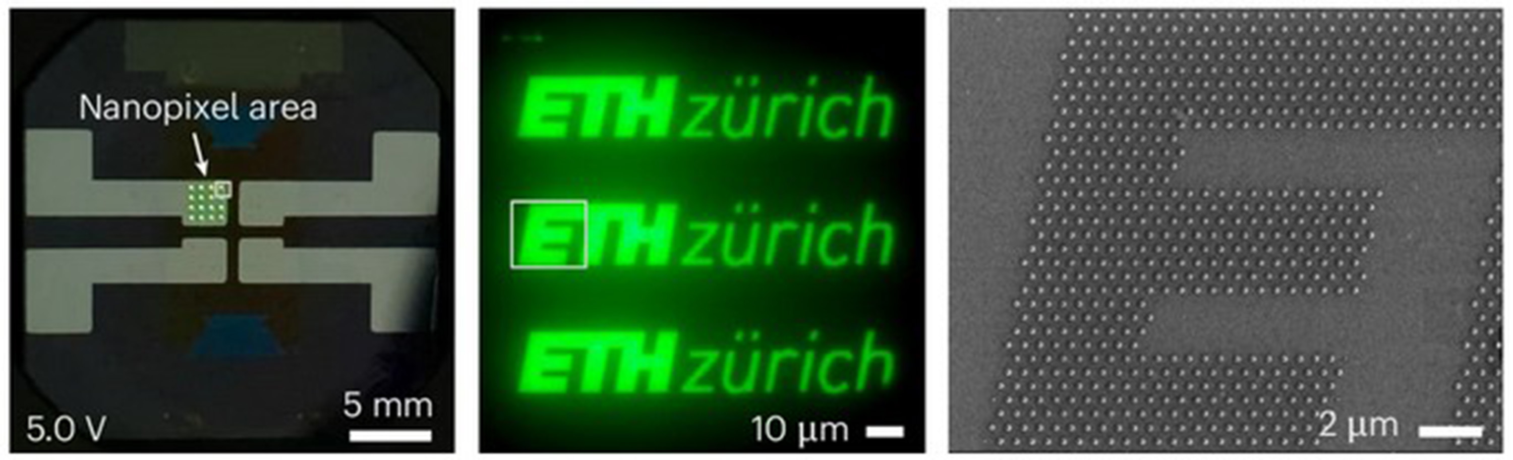
On the one hand, pixels ranging in size from 100 to 200 nanometres form the foundation for ultra-high-resolution screens that could display razor-sharp images in glasses worn close to the eye, for example. In order to illustrate this, Shih's team of researchers displayed the ETH Zurich logo. This ETH logo consists of 2,800 nano-OLEDs and is similar in size to a human cell, with each of its pixels measuring around 200 nanometres (0.2 micrometres). The smallest pixels developed so far by the ETH Zurich researchers reach the range of 100 nanometres.
Moreover, these tiny light sources could also help to focus on the sub-micrometre range by way of high-resolution microscopes. "A nano-pixel array as a light source could illuminate the most minute areas of a sample – the individual images could then be assembled on a computer to deliver an extremely detailed image," explains the professor of technical chemistry. He also perceives nano-pixels as potential tiny sensors that could detect signals from individual nerve cells, for example.
Nano-pixels generating optical wave effects
These minute dimensions also open up possibilities for research and technology that were previously entirely out of reach, as Marcato emphasises: "When two light waves of the same colour converge closer than half their wavelength – the so-called diffraction limit – they no longer oscillate independently of each other, but begin to interact with each other." In the case of visible light, this limit is between around 200 and 400 nanometres, depending on the colour – and the nano-OLEDs developed by the ETH researchers can be positioned this close together.
The basic principle of interacting waves can be aptly illustrated by throwing two stones next to each other into a mirror-smooth lake. Where the circular water waves meet, a geometric pattern of wave crests and troughs is created.
In a similar manner, intelligently arranged nano-OLEDs can produce optical wave effects in which the light from neighbouring pixels mutually reinforces or cancels each other out.
Manipulating light direction and polarisation
Conducting initial experiments, Shih's team was able to use such interactions to manipulate the direction of the emitted light in a targeted manner. Instead of emitting light in all directions above the chip, the OLEDs then only emit light at very specific angles. "In future, it will also be possible to bundle the light from a nano-OLED matrix in one direction and harness it to construct powerful mini lasers," Marcato expects.
Polarised light – which is light that oscillates in only one plane – can also be generated by means of interactions, as the researchers have already demonstrated. Today, this is at work in medicine, for example, in order to distinguish healthy tissue from cancerous tissue.
Modern radio and radar technologies give us an idea of the potential of these interactions. They use wavelengths ranging from millimetres to kilometres and have already been exploiting these interactions for some time. So-called phased array arrangements allow antennas or transmitter signals to be precisely aligned and focused.
In the optical spectrum, such technologies could, among other things, help to further accelerate the transmission of information in data networks and computers.
Ceramic membranes making all the difference
In the manufacture of OLEDs to date, the light-emitting molecules have been subsequently vapour-deposited onto the silicon chips. This is achieved by using relatively thick metal masks, which produce correspondingly larger pixels.
As Oh explains, the drive towards miniaturisation is now being enabled by a special ceramic material: "Silicon nitride can form very thin yet resilient membranes that do not sag on surfaces measuring just a few square millimetres."
Consequently, the researchers were able to produce templates for placing the nano-OLED pixels that are around 3,000 times thinner. "Our method also has the advantage that it can be integrated directly into standard lithography processes for the production of computer chips," as Oh underlines.
Opening a door to novel technologies
The new nano light-emitting diodes were developed within the context of Consolidator Grant awarded to Shih in 2024 by the Swiss National Science Foundation (SNSF). The researchers are currently working on optimising their method. In addition to the further miniaturisation of the pixels, the focus is also on controlling them.
"Our aim is to connect the OLEDs in such a way that we can control them individually," as Shih relates. This is necessary in order to leverage the full potential of the interactions between the light pixels. Among other things, precisely controllable nano-pixels could open the door to novel applications of phased array optics, which can electronically steer and focus light waves.
In the 1990s, it was postulated that phased array optics would enable holographic projections from two-dimensional screens. But Shih is already thinking one step ahead: in future, groups of interacting OLEDs could be bundled into meta-pixels and positioned precisely in space. "This would allow 3D images to be realised around viewers," says the chemist, with a look to the future.
Reference
Scalable nanopatterning of organic light-emitting diodes beyond the diffraction limit
Tommaso Marcato, Jiwoo Oh, Zhan-Hong Lin, Tian Tian, Abhijit Gogoi, Sunil B. Shivarudraiah, Sudhir Kumar, Ananth Govind Rajan, Shuangshuang Zeng & Chih-Jen Shih
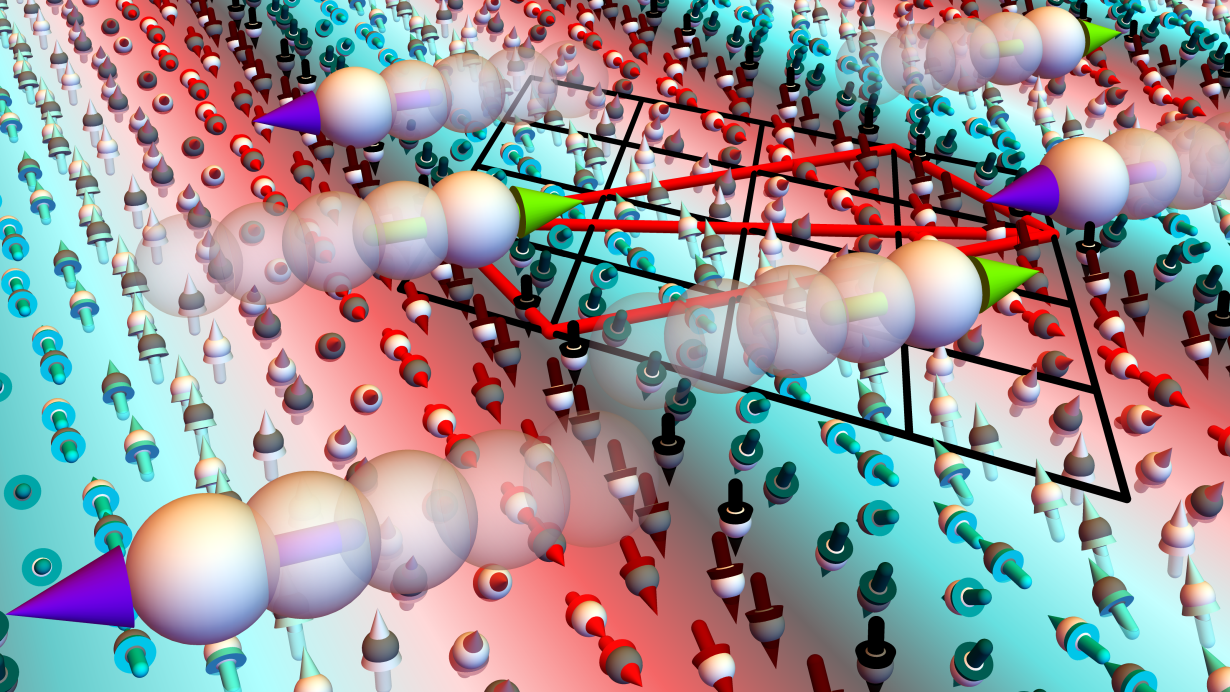
A novel magnetic material with an extraordinary electronic structure might allow for the production of smaller and more efficient computer chips in the future: the p-wave magnet. Researchers from Karlsruhe Institute of Technology (KIT) were involved in its development. The magnetic behavior in the interior of this material results from the way the electron spins arrange themselves – in the shape of a helix. Therefore, the electric current flowing through is deflected laterally. The results ar...
For a long time, the two areas of strong-field physics and quantum optics were considered independent areas of physics research without any significant overlaps. Whilst strong-field physics focuses on the behavior of material, such as atomic gases, in intense light fields, quantum optics focuses on researching special quantum properties of light that cannot be described within the framework of classical physics. Strong-field physics requires intense laser rays, in other words rays with innume...
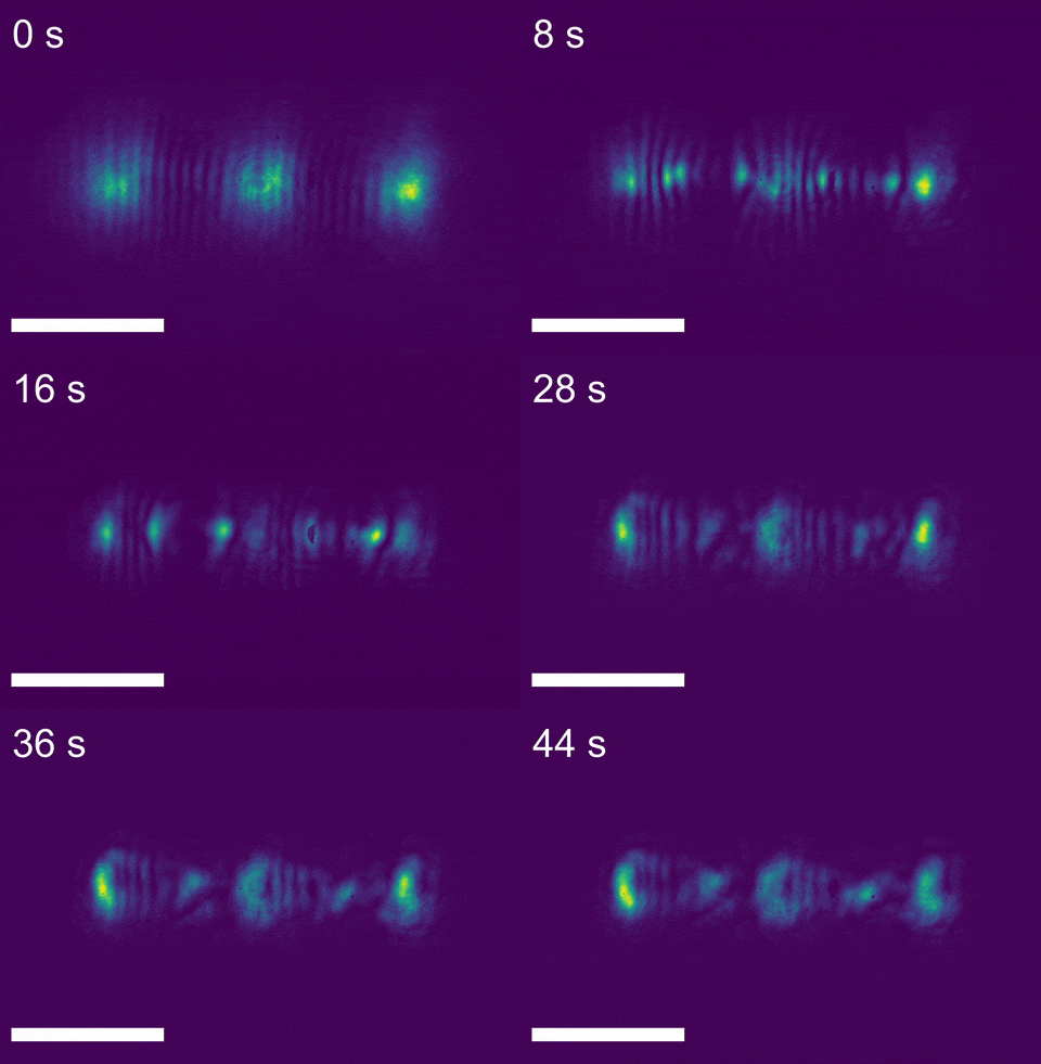
The group demonstrated that shining three self-trapped light beams into a specially engineered hydrogel can execute a NAND logic operation, one of the most fundamental building blocks of computing. Because all other digital logic gates can be built from NAND, the achievement establishes soft, photoresponsive materials as a realistic platform for autonomous, computation-capable systems.
This week in nanotech
$109M raised
3 funding rounds · 18 deals tracked
New products
 Nion-compatible In Situ STEM Holders for Electrical BiasingHummingbird Scientific Featured
 Ti-WCMBN Nanomaterialia Featured
 Discover Mapping SuiteOnto Innovation
Market insights
Last 30 days: Semiconductors & Electronics drew the most money: $545M.
Money raised per month