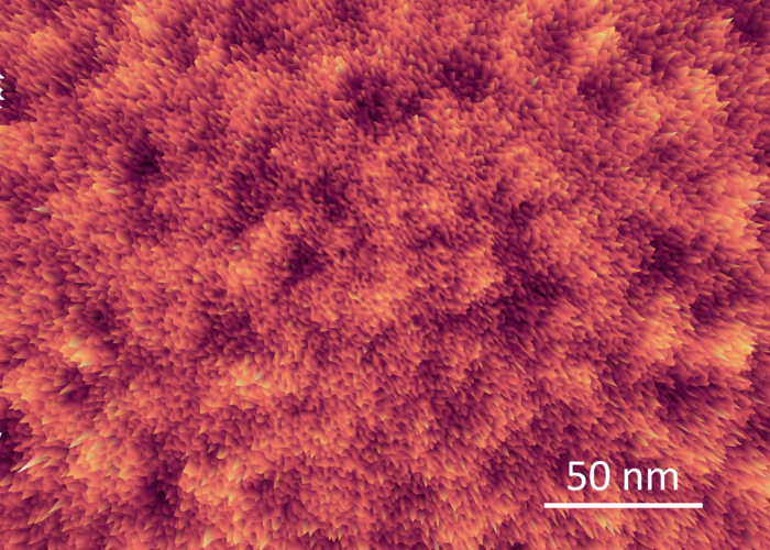
Researchers have analysed the properties of an organic polymer with potential applications in flexible electronics and uncovered variations in hardness at the nanoscale, the first time such a fine structure has been observed in this type of material.
The field of organic electronics has benefited from the discovery of new semiconducting polymers with molecular backbones that are resilient to twists and bends, meaning they can transport charge even if they are flexed into different shapes.
It had been assumed that these materials resemble a plate of spaghetti at the molecular scale, without any long-range order. However, an international team of researchers found that for at least one such material, there are tiny pockets of order within. These ordered pockets, just a few ten-billionths of a metre across, are stiffer than the rest of the material, giving it a ‘fruitcake’ structure with harder and softer regions.
The work was led by the University of Cambridge and Park Systems UK Limited, with KTH Stockholm in Sweden, the Universities of Namur and Mons in Belgium, and Wake Forest University in the USA. Their results, reported in the journal Nature Communications, could be used in the development of next-generation microelectronic and bioelectronic devices.
Studying and understanding the mechanical properties of these materials at the nanoscale – a field known as nanomechanics – could help scientists fine-tune those properties and make the materials suitable for a wider range of applications.
“We know that the fabric of nature on the nanoscale isn’t uniform, but finding uniformity and order where we didn’t expect to see it was a surprise,” said Dr Deepak Venkateshvaran from Cambridge’s Cavendish Laboratory, who led the research.
The researchers used an imaging technique called higher eigen mode imaging to take nanoscale pictures of the regions of order within a semiconducting polymer called indacenodithiophene-co-benzothiadiazole (C16-IDTBT). These pictures showed clearly how individual polymer chains line up next to each other in some regions of the polymer film. These regions of order are between 10 and 20 nanometres across.
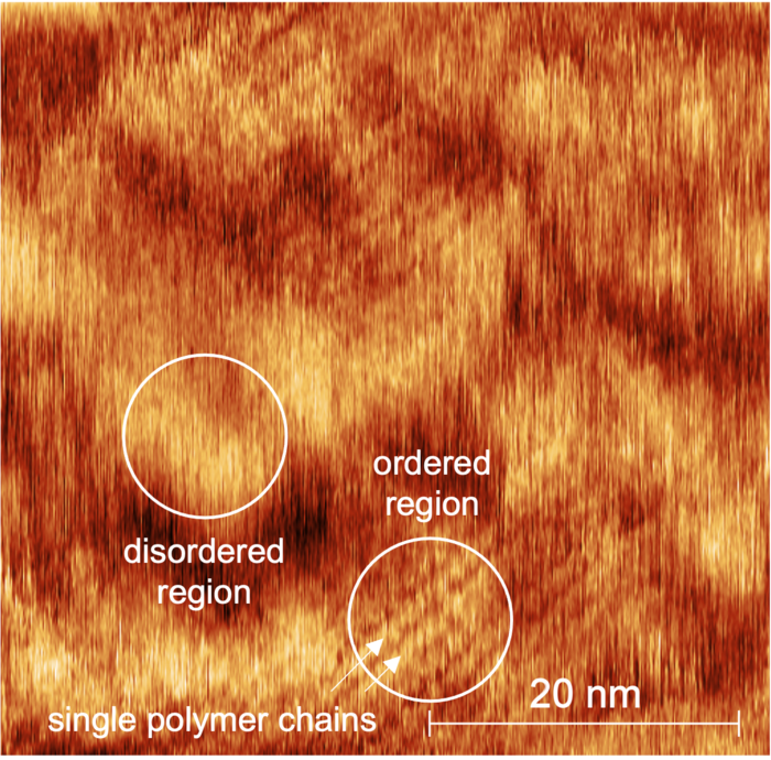
“The sensitivity of these detection methods allowed us to map out the self-organisation of polymers down to the individual molecular strands,” said co-author Dr Leszek Spalek, also from the Cavendish Laboratory. “Higher eigen mode imaging is a valuable method for characterising nanomechanical properties of materials, given the relatively easy sample preparation that is required.”
Further measurements of the stiffness of the material on the nanoscale showed that the areas where the polymers self-organised into ordered regions were harder, while the disordered regions of the material were softer. The experiments were performed in ambient conditions as opposed to an ultra-high vacuum, which had been a requirement in earlier studies.
“Organic polymers are normally studied for their applications in large area, centimetre scale, flexible electronics,” said Venkateshvaran. “Nanomechanics can augment these studies by developing an understanding of their mechanical properties at ultra-small scales with unprecedented resolutions.
“Together, the fundamental knowledge gained from both types of studies could inspire a new generation of soft microelectronic and bioelectronic devices. These futuristic devices will combine the benefits of centimetre scale flexibility, micrometre scale homogeneity, and nanometre scale electrically controlled mechanical motion of polymer chains with superior biocompatibility.”
Reference
Dynamic self-stabilization in the electronic and nanomechanical properties of an organic polymer semiconductor
Illia Dobryden, Vladimir V. Korolkov, Vincent Lemaur, Matthew Waldrip, Hio-Ieng Un, Dimitrios Simatos, Leszek J. Spalek, Oana D. Jurchescu, Yoann Olivier, Per M. Claesson & Deepak Venkateshvaran

Waste polyamide-derived CQDs show continuous photoluminescence tuning from 308 to 552 nm through sequential defect-state engineering, with optical transition energies decreasing from 4.32 to 2.50 eV. @Christian Ebere Enyoh from Saitama University Carbon quantum dots (CQDs) are fluorescent carbon nanomaterials with potential applications in sensing, optoelectronics, displays, anti-counterfeiting, and environmental technologies. Their optical properties can be adjusted by modifying the carbon...

The researchers used circularly polarized light at normal incidence and found that helicity-dependent photocurrents appeared perpendicular to the crystal’s polarization but vanished when measured parallel to it, supporting a bulk origin of CPGE. @Institute of Science Tokyo The circular photogalvanic effect (CPGE), a phenomenon that generates helicity-dependent photocurrents in noncentrosymmetric materials, can originate purely from a crystal's internal structure without contribution from the...

Summary of gold nanoparticle growth programming in liposome based on localization of biomineralization peptide The position of biomineralization peptides within liposomes can influence how gold nanoparticles grow, reports a research team from Institute of Science Tokyo. Peptides localized at the membrane interface promote branched structures, while those confined to the liposome interior favor spherical nanoparticles. The findings offer a new strategy for controlling nanoscale reaction...
