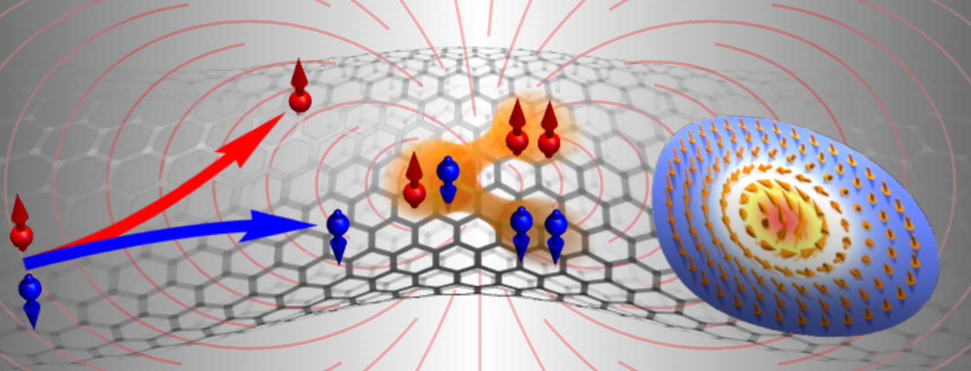
In a recently published paper in Nature Electronics, an international research group from Italy, Germany, the UK, and China examined significant development directions in the field of electronic materials with curved geometries at the nanoscale. From microelectronic devices with enhanced functionality to large-scale nanomembranes consisting of networks of electronic sensors that can provide improved performance.
The scientists argue that exciting developments induced by curvature at the nanoscale allow them to define a completely new field – curved nanoelectronics. The paper examines in detail the origin of curvature effects at the nanoscale and illustrates their potential applications in innovative electronic, spintronic and superconducting devices.
Curved solid-state structures also offer many application opportunities. On a microscopic level, shape deformations in electronic nanochannels give rise to complex three-dimensional spin textures with an unbound potential for new concepts in spin-orbitronics, which will help develop energy-efficient electronic devices. Curvature effects can also promote, in a semimetallic nanowire, the generation of topological insulating phases that can be exploited in nanodevices relevant for quantum technologies, like quantum metrology. In the case of magnetism, curvilinear geometry directly forges the magnetic exchange by generating an effective magnetic anisotropy, thus prefiguring a high potential for designing magnetism on demand.
Dr Ivan Vera-Marun from the National Graphene Institute at The University of Manchester commented: “nanoscale curvature and its associated strain result in remarkable effects in graphene and 2D materials. The development in preparation of high-quality extended thin films, as well as the potential to arbitrarily reshape those architectures after their fabrication, has enabled first experimental insights into how next-generation electronics can be compliant and thus integrable with living matter”.
The paper also describes the methods needed to synthesise and characterise curvilinear nanostructures, including complex 3D nanoarchitectures like semiconductor nanomembranes and rolled up sandwiches of 2D materials, and highlights key areas for the future developments of curved nanoelectronics.
Reference
Electronic materials with nanoscale curved geometries
Paola Gentile, Mario Cuoco, Oleksii M. Volkov, Zu-Jian Ying, Ivan J. Vera-Marun, Denys Makarov & Carmine Ortix
https://www.nature.com/articles/s41928-022-00820-z

Waste polyamide-derived CQDs show continuous photoluminescence tuning from 308 to 552 nm through sequential defect-state engineering, with optical transition energies decreasing from 4.32 to 2.50 eV. @Christian Ebere Enyoh from Saitama University Carbon quantum dots (CQDs) are fluorescent carbon nanomaterials with potential applications in sensing, optoelectronics, displays, anti-counterfeiting, and environmental technologies. Their optical properties can be adjusted by modifying the carbon...

The researchers used circularly polarized light at normal incidence and found that helicity-dependent photocurrents appeared perpendicular to the crystal’s polarization but vanished when measured parallel to it, supporting a bulk origin of CPGE. @Institute of Science Tokyo The circular photogalvanic effect (CPGE), a phenomenon that generates helicity-dependent photocurrents in noncentrosymmetric materials, can originate purely from a crystal's internal structure without contribution from the...

Summary of gold nanoparticle growth programming in liposome based on localization of biomineralization peptide The position of biomineralization peptides within liposomes can influence how gold nanoparticles grow, reports a research team from Institute of Science Tokyo. Peptides localized at the membrane interface promote branched structures, while those confined to the liposome interior favor spherical nanoparticles. The findings offer a new strategy for controlling nanoscale reaction...
