Karlsruhe Institute of Technology (KIT)
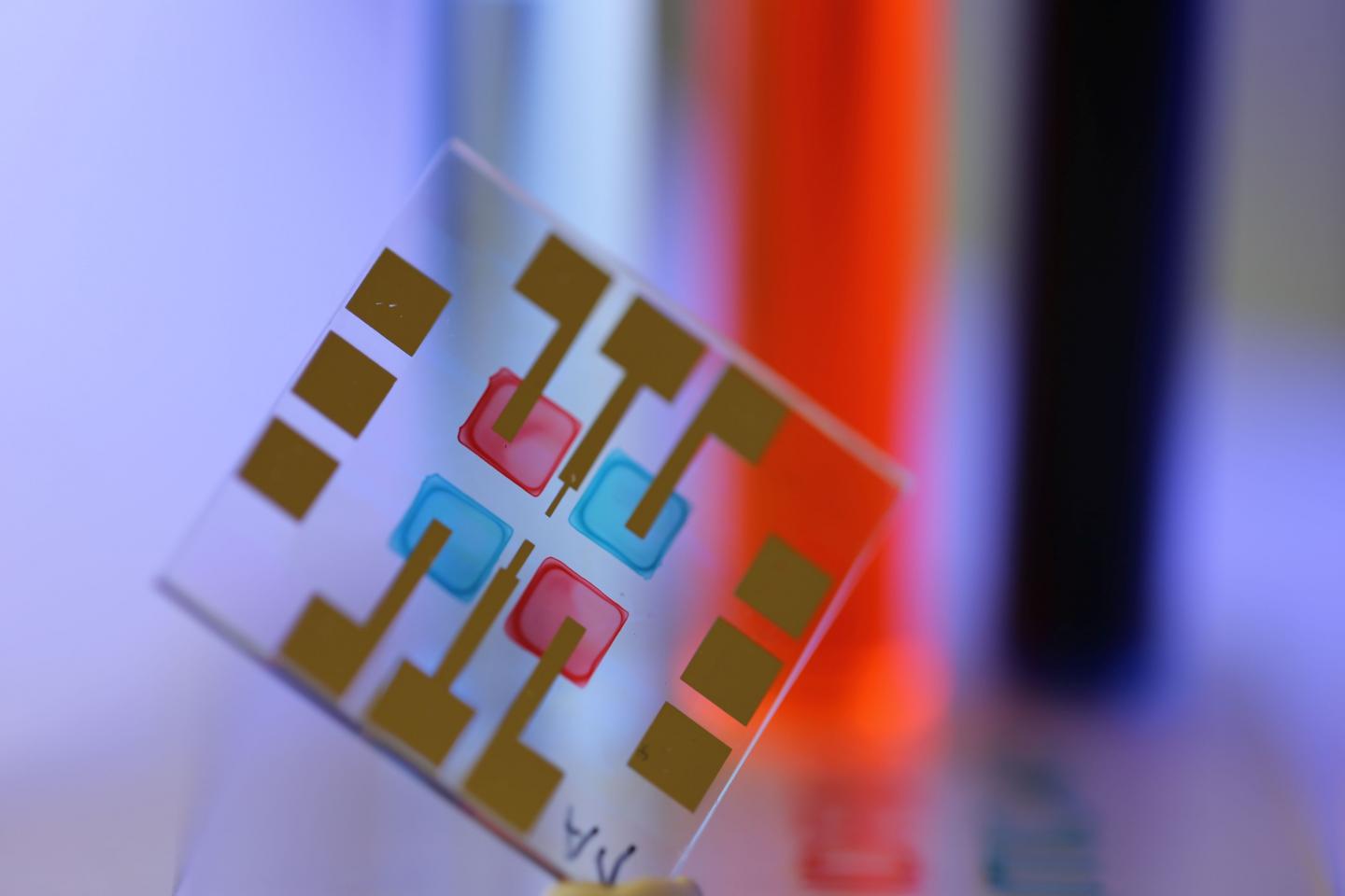
Cameras, light barriers, and movement sensors have one thing in common: They work with light sensors that are already found in many applications. In future, these sensors might also play an important role in telecommunications, as they enable data transmission via light. At the InnovationLab in Heidelberg, scientists of Karlsruhe Institute of Technology (KIT) succeeded in making decisive progress: Printable light sensors that can see colors. The results are now reported in Advanced Materials (DOI: 10.1002/adma.201908258).
New technologies will increase the demand for optical sensors for a variety of applications, including visible light communication (VLC). VLC uses interior lighting of buildings for optical communication. In terms of security, speed, and accessibility, this technology has a number of advantages over conventional transmission processes, such as WLAN or Bluetooth. "Our research is based on the idea of combining the advantages of a special type of materials, namely, organic semiconductors, and their production by printing processes," says Dr. Gerardo Hernandez-Sosa of KIT's Light Technology Institute, one of the authors of the publication.
Semiconductors are the basis of computers, smartphones, solar cells, and many other technologies. Some of the semiconducting materials react to light by changing their conductivity. Light intensity can be measured as electrical current. Using a printer, some materials can be applied to a carrier material like printing ink. These materials react to varying wavelengths, which means that they can distinguish colors. The team of Hernandez-Sosa has now succeeded in finding a composition of materials suited for use as wavelength-sensitive light detector as well as for printing onto flexible carriers. Printing can be performed on very small to very large areas. The layout can be designed easily with the help of a computer. "High numbers of these photodetectors of any design can be produced on flexible, light materials. Hence, they are particularly suited for mobile devices," first author Noah Strobel points out.
Printing of semiconductor components is a relatively young process, but has a considerable potential for future applications. Industry is already making large investments in the production of printed OLED displays for TVs and smartphones. Printed flexible solar cells or pressure sensors are commercially available already. Production of printed light detectors has also reached the industrial scale. It is therefore highly probable that these elements will be used in many applications in future, even more so, as the demand for sensors is increasing in the internet of things, in smart cities, and in Industry 4.0.
Color-selective Printed Organic Photodiodes for Filterless Multichannel Visible Light Communication
Noah Strobel, Nikolaos Droseros, Wolfgang Köntges, Mervin Seiberlich, Manuel Pietsch, Stefan Schlisske, Felix Lindheimer, Rasmus R. Schröder, Uli Lemmer, Martin Pfannmöller, Natalie Banerji, Gerardo Hernandez-Sosa
Advanced Materials, 2020
Contact information:
Head of BMBF Junior Research Group "BioLicht"
gerardo.sosa@kit.edu
Phone: +49 6221 54 19134
Printed Electronics Group at InnovationLab

Waste polyamide-derived CQDs show continuous photoluminescence tuning from 308 to 552 nm through sequential defect-state engineering, with optical transition energies decreasing from 4.32 to 2.50 eV. @Christian Ebere Enyoh from Saitama University Carbon quantum dots (CQDs) are fluorescent carbon nanomaterials with potential applications in sensing, optoelectronics, displays, anti-counterfeiting, and environmental technologies. Their optical properties can be adjusted by modifying the carbon...

The researchers used circularly polarized light at normal incidence and found that helicity-dependent photocurrents appeared perpendicular to the crystal’s polarization but vanished when measured parallel to it, supporting a bulk origin of CPGE. @Institute of Science Tokyo The circular photogalvanic effect (CPGE), a phenomenon that generates helicity-dependent photocurrents in noncentrosymmetric materials, can originate purely from a crystal's internal structure without contribution from the...

Summary of gold nanoparticle growth programming in liposome based on localization of biomineralization peptide The position of biomineralization peptides within liposomes can influence how gold nanoparticles grow, reports a research team from Institute of Science Tokyo. Peptides localized at the membrane interface promote branched structures, while those confined to the liposome interior favor spherical nanoparticles. The findings offer a new strategy for controlling nanoscale reaction...
