Vienna University of Technology
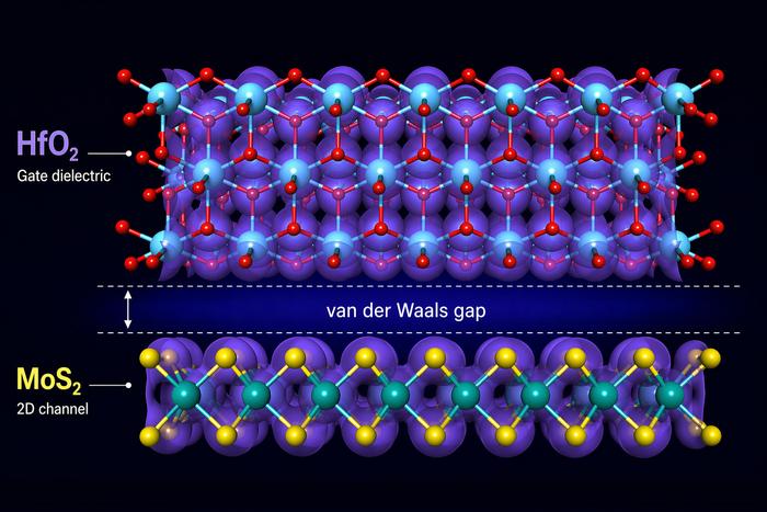
The miniaturization of electronic components has been a tremendous success story, driving technological progress for decades. Work is already underway on the next revolution in computer chips: 2D materials—ultrathin layers consisting of just one or a few atomic layers—could be ideally suited for even smaller electronic structures.
However, researchers at TU Wien have now shown that many 2D materials once considered highly promising are in fact unsuitable for this purpose. It is not enough to study the properties of the material itself—interface effects must also be taken into account. When 2D materials are combined with an insulating layer, an extremely thin gap inevitably forms between them, drastically degrading their electronic properties. The good news is that this approach also allows researchers to identify which materials are not affected by this problem—potentially saving the semiconductor industry from investing billions in technologies that are fundamentally limited by the laws of physics.
“For many years, researchers have quite rightly been fascinated by the remarkable electronic properties of novel 2D materials such as graphene or molybdenum disulfide,” says Prof. Mahdi Pourfath, who carried out the research together with Prof. Tibor Grasser at TU Wien’s Institute for Microelectronics. “What is often overlooked, however, is that a 2D material alone does not make an electronic device. We also need an insulating layer—usually an oxide. And this is where things become more complicated from a materials science perspective.”
The basic concept of transistors used in computer chips is simple: the conductivity of a semiconductor—this can also be an ultrathin 2D material—can be modulated between conducting and non-conducting states. Which of these states occurs is controlled by the gate, an electrode that must be separated from the active material by an insulating layer.
This insulating layer must be as thin as possible in order to allow precise control of the electric fields in the 2D material, enabling extremely small and compact devices. However, when these structures are analyzed at the atomic scale, a problem emerges that has so far received little attention.
“In many combinations of 2D materials and insulating layers, the bonding between them is relatively weak,” explains Grasser. “They are held together only by so-called van der Waals forces, which provide only a weak attraction between the semiconductor and the insulator. As a result, the two layers do not come into close contact—there is always a gap between them.”
This gap is tiny—only about 0.14 nanometers, thinner than a single sulfur atom—yet it has a major impact on electronic performance. A SARS-CoV-2 virus, for comparison, is roughly 700 times larger. “This gap weakens the capacitive coupling between the layers. No matter how good the intrinsic properties of the materials may be, the gap can become the limiting factor. As long as it exists, it imposes a fundamental limit on how far these devices can be miniaturized.”
“If the semiconductor industry wants to succeed with 2D materials, the active layer and the insulating layer must be designed together from the very beginning,” emphasizes Mahdi Pourfath. There are possible solutions: so-called “zipper materials” combine both aspects. Semiconductor and insulator interlock with each other—they are not just loosely connected by van der Waals forces, but form a stronger bond that eliminates the gap.
“Our work is good news for the semiconductor industry,” says Tibor Grasser. “We can predict which materials are suitable for future miniaturization steps—and which are not. But if one focuses only on the 2D materials themselves, without considering the unavoidable insulating layers from the outset, there is a risk of investing billions in an approach that simply cannot succeed for fundamental physical reasons.”
Reference
Device-scaling constraints imposed by the van der Waals gap formed in two-dimensional materials
Mahdi Pourfath and Tibor Grasser

Rice University researchers studying a class of atom-thin semiconductors known as transition metal dichalcogenides (TMDs) have discovered that light can trigger a physical shift in their atomic lattice, creating a tunable way to adjust the materials’ behavior and properties. The effect, observed in a TMD subtype named after the two-faced Roman god of transitions, Janus, could advance technologies that use light instead of electricity, from faster and cooler computer chips to ultrasensitive se...
A team led by Lawrence Berkeley National Laboratory (Berkeley Lab) and George Washington University have confirmed that atoms in semiconductors will arrange themselves in distinctive localized patterns that change the material’s electronic behavior. The research, published today in Science, may provide a foundation for designing specialized semiconductors for quantum-computing and optoelectronic devices for defense technologies. On the atomic scale, semiconductors are crystals made of differe...

Self-driving cars which eliminate traffic jams, getting a healthcare diagnosis instantly without leaving your home, or feeling the touch of loved ones based across the continent may sound like the stuff of science fiction. But new research, led by the University of Bristol and published in the journal Nature Electronics, could make all this and more a step closer to reality thanks to a radical breakthrough in semiconductor technology.
This week in nanotech
$10.2M raised
2 funding rounds · 18 deals tracked
New products
 Nion-compatible In Situ STEM Holders for Electrical BiasingHummingbird Scientific Featured
 DLS-1 Mass Spectrometer for Fusion Gas AnalysisHiden Analytical Featured
 NanoFlow® S1-20Levidian
Market insights
Last 30 days: Quantum Technologies was the busiest vertical: 52 of 174 events (30%).
Money raised per month