14 September 2026. MSE Supplies LLC published an article on September 14, 2026, by Joem Viyar, stating that dislocation density in grown diamond substrates is inherited from the seed plate, not generated by the reactor. The article compares CVD and HPHT growth methods and argues that seed qualification is more important than the choice between them.
The article says threading dislocations in a seed plate propagate vertically into a homoepitaxial CVD layer. Growth does not anneal them out; it extends them layer after layer. Subsurface damage from seed preparation introduces strained lattice regions that nucleate stacking faults and secondary dislocations at the growth interface.
X-ray topography studies of homoepitaxial CVD layers on {001} substrates have traced a specific subset of defects, 45-degree mixed dislocations, to substrate polishing damage. The same work found that dislocation density at the interface can be held below 400 cm⁻² when high-quality type IIa HPHT substrates are used as the seed. Commercial type Ib HPHT diamond runs 10³ to 10⁶ dislocations per cm² depending on size, while higher-grade type IIa material can reach as low as 10³ cm⁻².
For CVD, the article states that sub-nanometer RMS surface roughness is a practical requirement for homoepitaxial seeds, because residual roughness drives non-uniform nucleation and step-bunching. It also notes that off-axis miscut angle affects growth: too shallow a miscut promotes three-dimensional nucleation, and too steep increases defect incorporation. Heteroepitaxial growth on iridium, silicon carbide, or silicon introduces a defect floor from lattice mismatch and thermal expansion differences, independent of seed quality.
The article recommends requesting dislocation density figures (etch pit density or X-ray topography data), a defined miscut angle tolerance, and a stated subsurface damage depth from polishing before a growth run. It states that these are not standard line items on most seed plate quotes.
"The real question isn't CVD versus HPHT—it's whether the seed was qualified before either process began."
Source: MSE Supplies LLC news
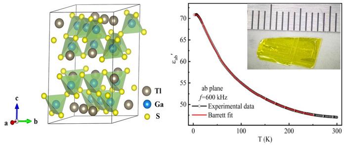
TlGaS2 single crystals show both in-plane and out-of-plane polarization, a rare combination in two-dimensional ferroelectrics that could widen options for ferroelectric transistors and non-volatile memory. Infrared spectroscopy revealed a soft phonon mode below 75 K, a signature tied to quantum ferroelectricity, along with weak structural changes across temperatures that lack clear heat-capacity signals, hinting at local rearrangements rather than conventional phase transitions.
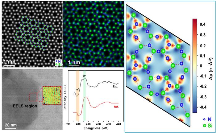
A β-Si3N4 nanolayer about 20 nm thick and continuous over several micrometers has been formed between carbon and silicon carbide without conventional oxide sintering additives, using a porous carbon framework infiltrated with molten silicon. Complementary atomic-resolution imaging resolved both silicon and nitrogen sublattices, confirming the ABAB stacking and corner-sharing tetrahedral network, while electron energy-loss spectroscopy and first-principles calculations linked the spectra to…
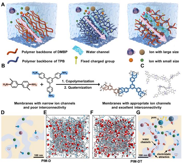
A polymer membrane with interconnected water-filled channels just 0.5 to 0.7 nanometers wide separates singly charged ions from multiply charged ones in both cationic and anionic systems. Built from Tröger's base-derived porous organic polymers, it cut the magnesium-to-lithium ratio in salt-lake brine roughly 500-fold across three electrodialysis stages, yielding 99.5 percent pure lithium carbonate, and enriched sodium chloride to 99.4 percent of ion mass from simulated seawater.
This week in nanotech
$555M raised
5 funding rounds · 34 deals tracked
New products
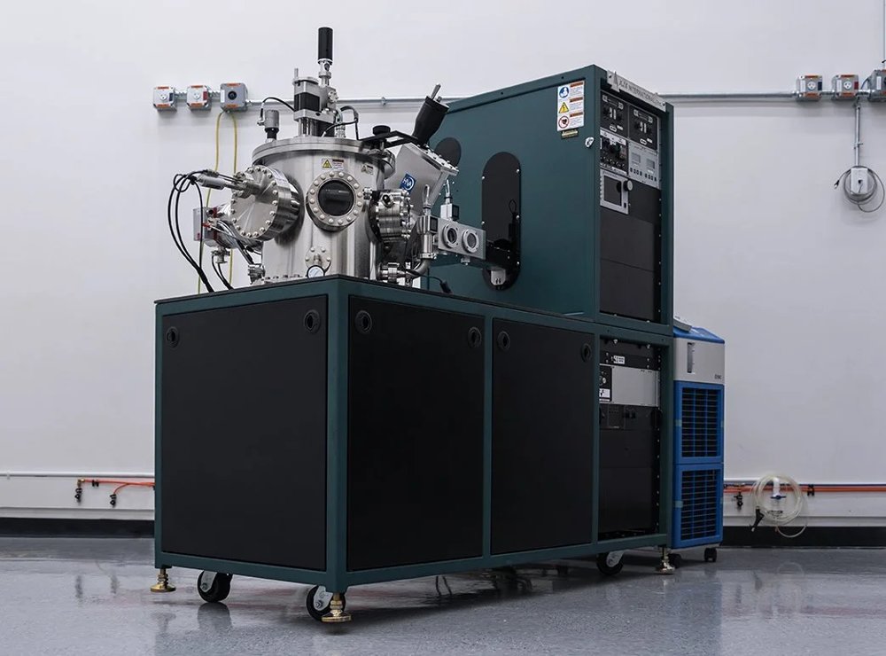 Orion Sputtering Deposition SystemsAJA International Featured
 Ti-WCMBN Nanomaterialia Featured
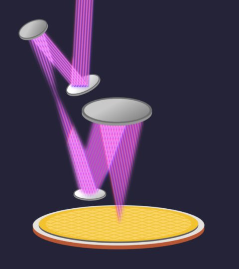 Aether®Lam Research
Market insights
Last 30 days: Quantum Technologies drew the most money: $2.15B.
Money raised per month