30 September 2026. NanoImages, LLC has published details of its electron-beam-induced current (EBIC) imaging technique for semiconductor failure analysis. The company says EBIC measures the current flowing through a sample rather than the electrons or X-rays emitted from it, producing an image of where the electronics work.
In EBIC, each primary electron generates thousands of electron-hole pairs, the company states. Creating one pair costs roughly three times the bandgap energy, so a 20 keV electron landing in silicon produces on the order of five thousand of them. Near a p-n junction or Schottky contact, the built-in electric field separates the carriers. A picoampere beam becomes nanoamperes of collected signal, an amplification factor of a few thousand.
The company lists recombination centers including dislocations, stacking faults, grain boundaries, metallic precipitates, and process-induced damage. These appear as dark spots, lines, and boundaries on a bright background.
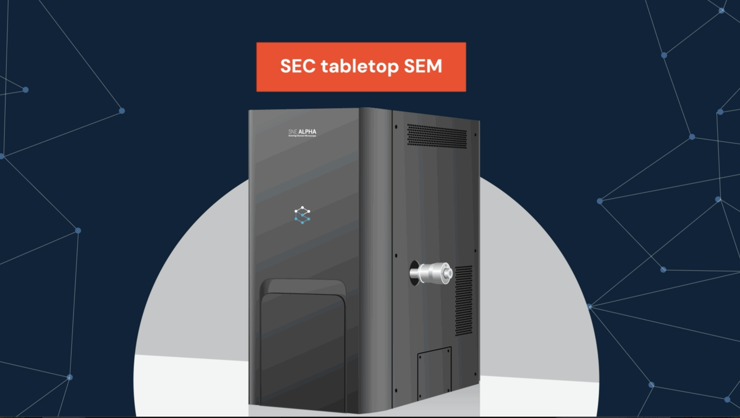
The SNE-Alpha carries a factory EBIC port alongside its EDS, EBSD, Raman, and CL ports, with a 1-30 kV range. NanoImages notes that packaged parts need decapsulation, and that thick passivation may call for higher kV or careful thinning.
Source: NanoImages, LLC news
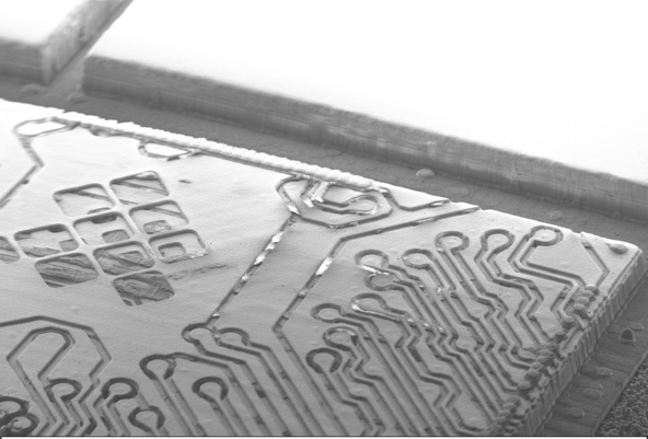
TESCAN ORSAY HOLDING, a.s. has described an A15 semiconductor failure analysis workflow that connects X-ray CT, ultrafast laser processing, optical and confocal microscopy, and SEM for progressive access to buried structures.
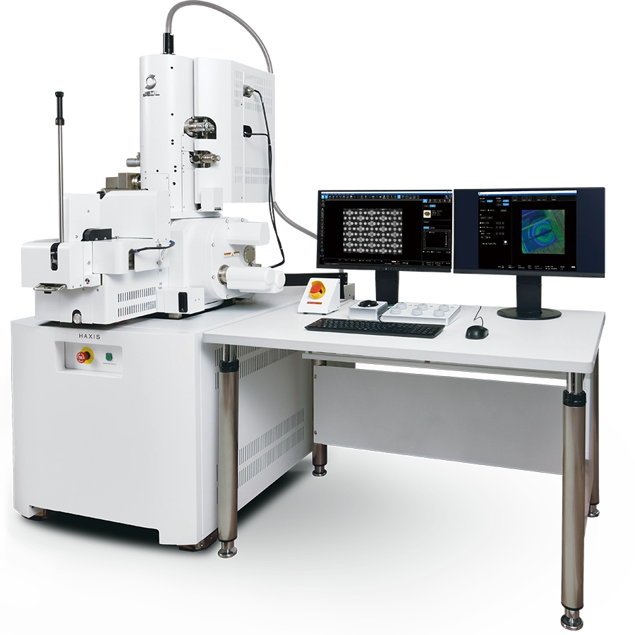
JEOL has started sales of HAXIS, a scanning electron microscope with low-angle argon ion milling and passive voltage contrast detection, for layer-by-layer semiconductor failure analysis.
Fraunhofer IZM and Swissbit described Europe's advanced packaging gap between pilot production and mass manufacturing. Fraunhofer's Rolf Aschenbrenner and Swissbit's Lars Lust said low volumes such as 20 to 100 wafers per year are too small for large OSAT providers.