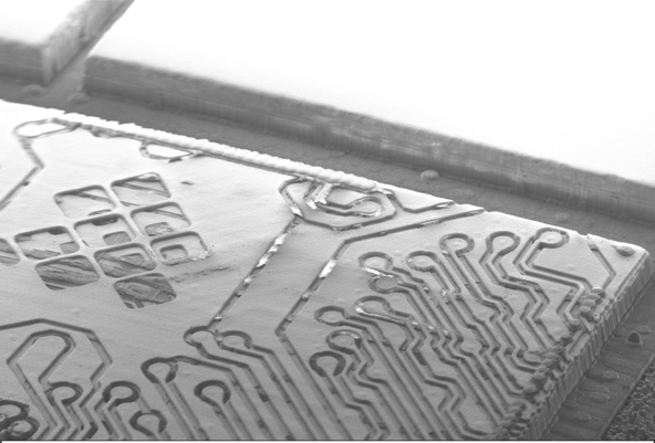
7 October 2026. TESCAN ORSAY HOLDING, a.s. has described a semiconductor failure analysis workflow that connects nondestructive X-ray computed tomography (CT), ultrafast laser processing, optical and confocal microscopy, and scanning electron microscopy (SEM). The A15 workflow is shown in a webinar on a cryo-EM solution for beam-sensitive materials using Tescan TENSOR.
The workflow begins with X-ray CT of an intact smartphone. The three-dimensional CT volume provides a navigation map for locating the A15 package, understanding its orientation and surrounding structures, and planning an access path before destructive preparation begins.
Tescan FemtoChisel is then used for controlled laser decapsulation and overburden removal, exposing package-level features of DRAM circuitry and adjacent silicon structures. Sequential laser delayering removes the upper DRAM circuitry, exposing the underlying silicon. Processing continues through the DRAM-associated silicon, revealing a second buried DRAM pair and reaching the interposer metallization. Multiple copper levels are then exposed step by step.
Microscopy guides the decisions between laser-processing steps. Optical microscopy documents large-area geometry and exposed features. Confocal microscopy provides three-dimensional surface topography and depth information. SEM adds higher-resolution inspection of exposed circuitry, interfaces, and local structural details.
The company states that for advanced packaging failure analysis, reliability investigations, and security-oriented inspection, the value of an exposed feature increases when it can be related to its position within the original device.
Source: TESCAN ORSAY HOLDING, a.s. news
Fraunhofer IZM and Swissbit described Europe's advanced packaging gap between pilot production and mass manufacturing. Fraunhofer's Rolf Aschenbrenner and Swissbit's Lars Lust said low volumes such as 20 to 100 wafers per year are too small for large OSAT providers.
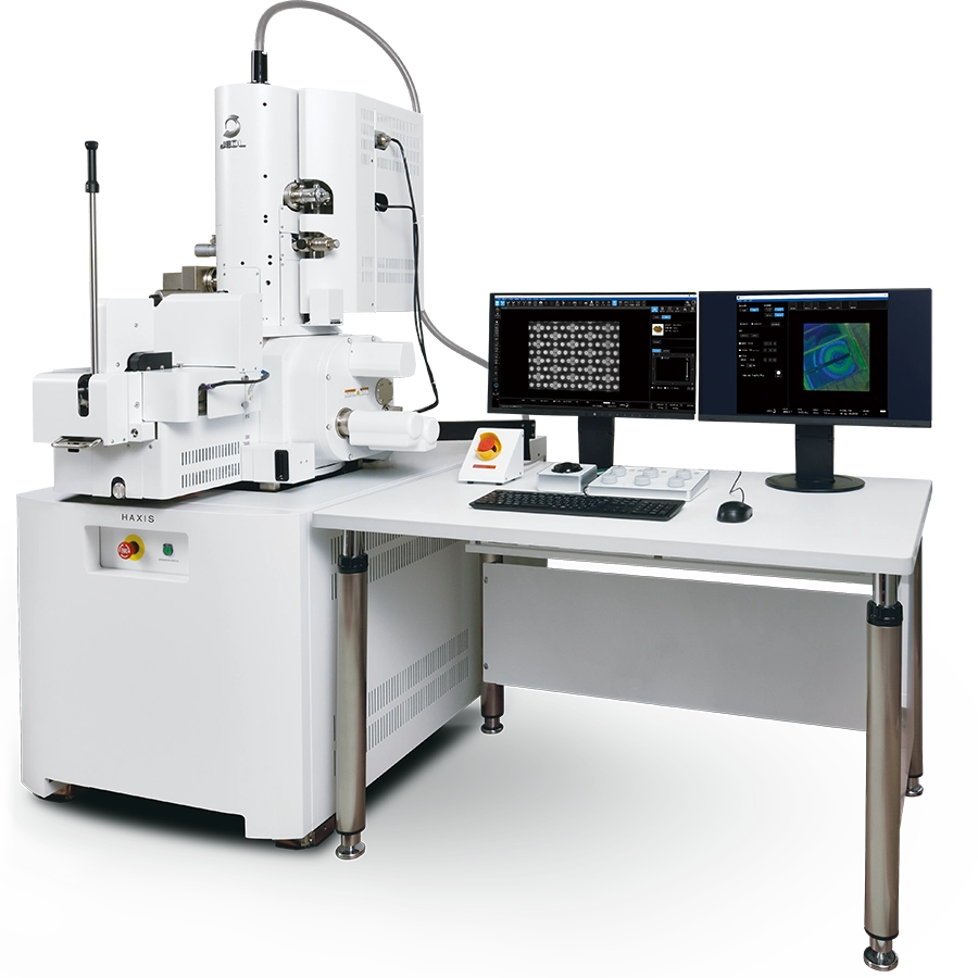
JEOL has started sales of HAXIS, a scanning electron microscope with low-angle argon ion milling and passive voltage contrast detection, for layer-by-layer semiconductor failure analysis.
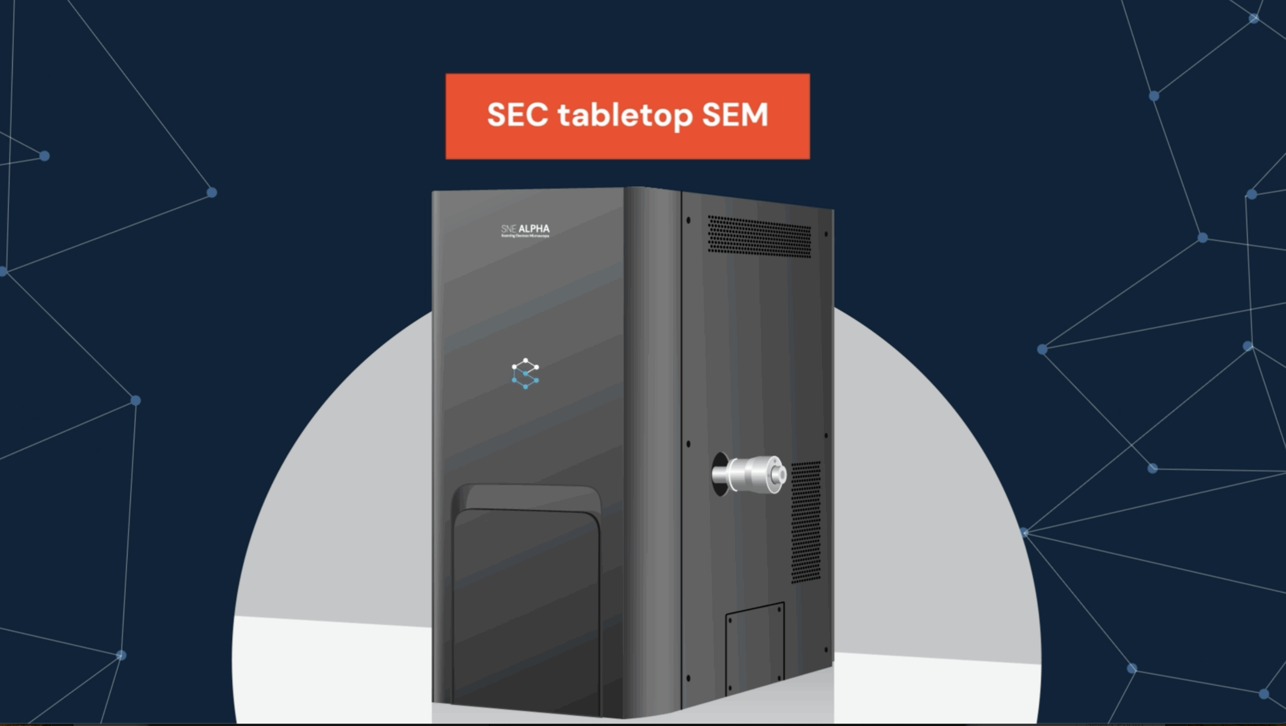
NanoImages, LLC has published details of its EBIC imaging technique for semiconductor failure analysis. The SNE-Alpha carries a factory EBIC port alongside its EDS, EBSD, Raman, and CL ports, with a 1-30 kV range.