Institute for Basic Science (IBS)
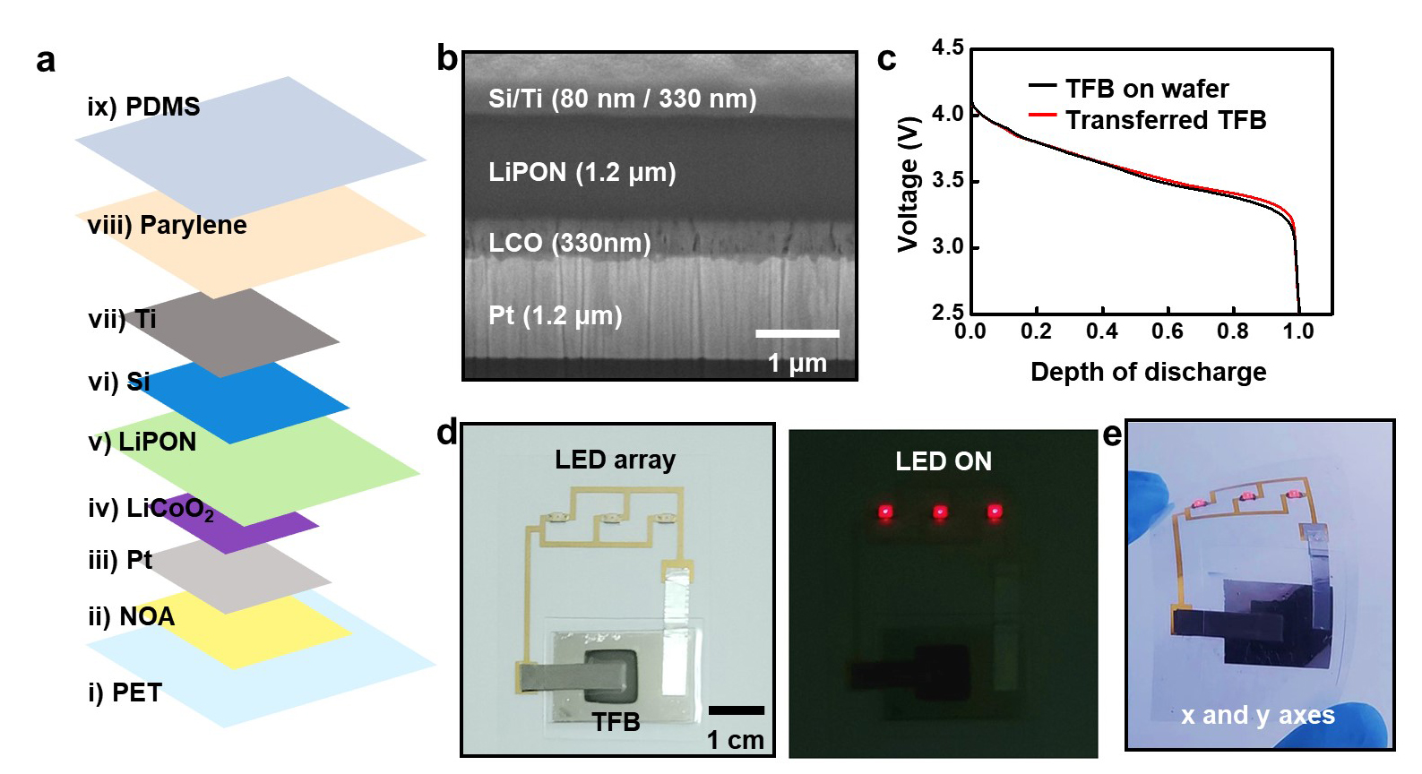
Researchers at the Institute for Basic Science (IBS), South Korea, have developed an innovative dry transfer printing technique for flexible electronic devices. This method, spearheaded by Prof. KIM Dae-Hyeong, Dr. LEE Sangkyu, (IBS Center for Nanoparticle Research), and Prof. KIM Jihoon (Pusan University), allows for the transfer of high-quality electronic materials without damage, a significant advancement in the field.
Typically, high-quality electronic materials are synthesized and processed at high temperatures to achieve the necessary crystalline structures and electrical properties. These high temperatures, however, make it challenging to process such materials directly on flexible or stretchable substrates. Hence for building flexible/stretchable devices, the electronics must be “transfer printed” from solid to soft substrate. Existing transfer printing technologies issues such as the use of toxic chemicals and potential mechanical damage during the transfer process.
To address this issue, various methods such as laser or thermal processes and delamination in water have been developed. However, these methods require expensive equipment, involve additional post-processing, or are limited to specific environments. Additionally, it is challenging to use conventional transfer printing for high-quality electronic materials that require high-temperature treatment to form crystalline structures.
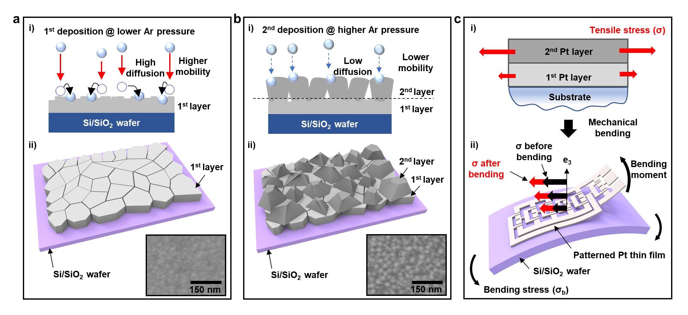
To overcome these challenges, the research team developed a damage-free dry transfer printing method that controls stress within thin films. This new method allows metal and oxide thin films, processed at high temperatures, to be transferred to flexible substrates without damage. By adjusting sputtering parameters, the team controlled the type and magnitude of stress within the thin film. They created bilayer structures with varying stresses to maximize the stress gradient and applied additional tensile stress through external bending deformation. This process maximizes the strain energy release rate, allowing reliable delamination by surpassing the interfacial strength between the thin film and the substrate.
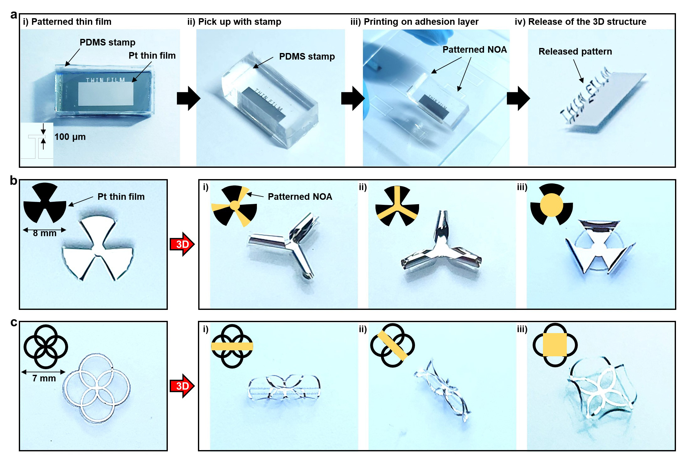
"Our transfer method avoids toxic substances, minimizes device damage, and eliminates the need for post-processing, resulting in shorter transfer times," said Dr. SHIN Yoonsu, first co-author. "It can transfer large areas as well as micro-scale patterns, making it highly versatile."
The team demonstrated that greater stress gradients within thin films result in larger bending moments, causing them to curl and transform from a two-dimensional (2D) thin film into a three-dimensional (3D) structure. The configuration of 3D structures can be adjusted by the pattern of the adhesive layer during transfer printing, allowing for the design and fabrication of desired structures to meet various requirements.
Dr. LEE Sangkyu, one of the corresponding authors, emphasized, "The key to this research is the development of a damage-free dry transfer printing technique by controlling only material properties, unlike previous studies." He added, "We plan to further research the fabrication of diverse 3D devices, leveraging the technology to transform 2D thin films into 3D structures, beyond the simple 2D flexible battery devices demonstrated in the paper."
"Transfer printing technology has applications across fields such as flexible electronics, optoelectronics, bioelectronics, and energy devices. Our method offers significant advantages for producing high-density 2D and 3D functional thin film structures without damage, greatly benefiting the development of new high-performance electronic devices," remarked Prof. KIM Dae-Hyeong.
Reference
Damage-free dry transfer method using stress engineering for high-performance flexible two- and three-dimensional electronics
Yoonsoo Shin, Seungki Hong, Yong Chan Hur, Chanhyuk Lim, Kyungsik Do, Ji Hoon Kim, Dae-Hyeong Kim & Sangkyu Lee
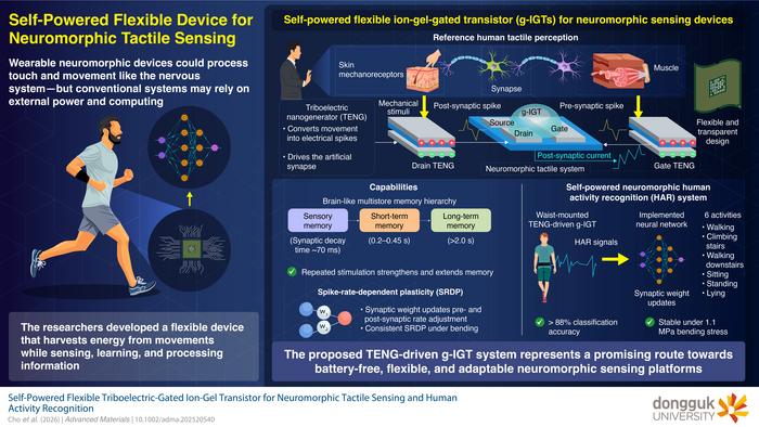
The proposed TENG-driven g-IGT is a flexible, self-powered neuromorphic device capable of reproducing multiple memory states and spike-rate-dependent learning Neuromorphic devices, which are designed to emulate aspects of biological neural networks, are promising candidates for developing low-power and intelligent sensing technologies, including wearable applications. Among the device architectures explored for neuromorphic computing, graphene-channel ion-gel-gated transistors (g-IGTs) are...
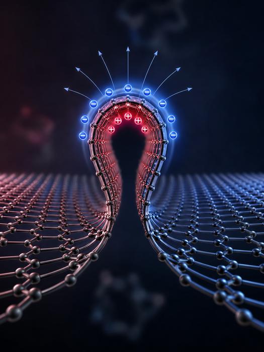
Rice University researchers have shown that sub-nanometer wrinkles in graphene generate flexoelectric charge separation, reshaping local electrical behavior through curvature alone. Extreme bending produces polarization far stronger than in larger systems and may enable geometry-controlled electronics without chemical doping. Published in Advanced Materials.
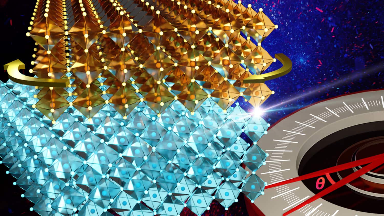
Researchers at NC State have extended twistronics beyond van der Waals materials into strongly bonded crystalline oxides. By stacking sodium niobate membranes with twist angles controlled down to 0.1 degrees, and confirming results via synchrotron X-ray diffraction, the team found interlayer bonds distort the atomic lattice, shifting phase structure and domain configuration. The technique works at near-millimeter scale, far larger than typical twistronic devices, marking a real step toward pract
