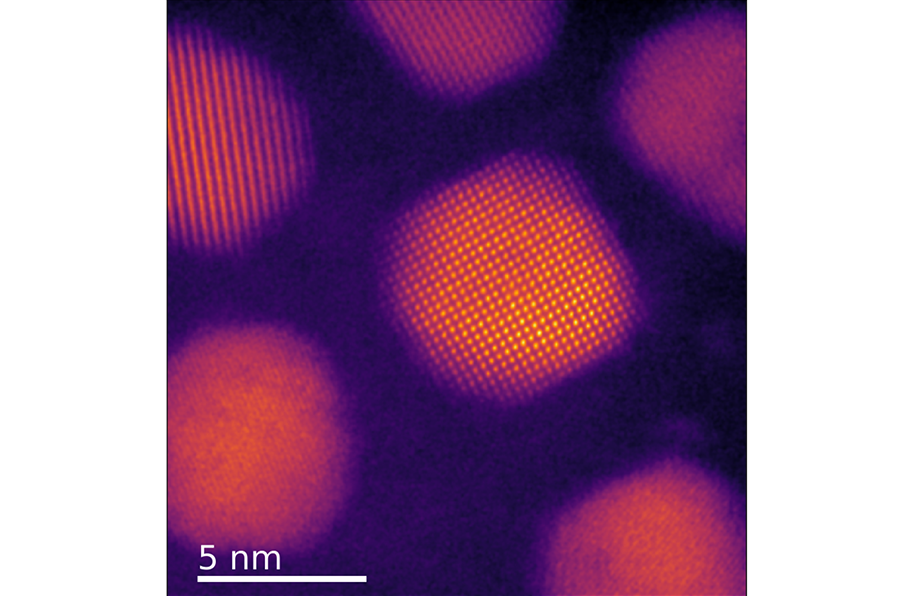
Creating new quantum technologies has historically been a trade-off, with researchers often forced to choose between building a sensitive device or a robust one.
This issue has become more pressing as quantum information technology stands poised to revolutionize communication and computing, with potential applications for everything from medicine and biology to optoelectronics and catalysis.
“One of the big problems that's going on in quantum information today, and people trying to make real technology with it, is figuring out how to integrate it with many different systems,” said Joeson Wong, a postdoctoral researcher in the UChicago Pritzker School of Molecular Engineering’s Alivisatos Lab.
Spin defects inside diamonds and other crystals make ideal qubits – the building block of quantum devices. However, if the defect is too deep inside the crystal, it’s harder to integrate the qubit into the device. If the defect is too close to the material’s surface, it’s vulnerable to all sorts of electric and magnetic noise, reducing the qubit’s effectiveness.
Wong is first author of a paper recently published in ACS Nano that has found a solution to this longstanding problem. In the paper, a UChicago PME-led team of researchers from UChicago, Argonne National Laboratory and University of Illinois Chicago used defect-embedded colloidal nanocrystals to create a perfect mixture of tiny solids in solution. It’s a material in which the qubits are both close to the surface and protected from noise – a material both sensitive and robust.
“This way, we create a system that is intrinsically almost all surface but has the kind of modularity that you might want for technology,” Wong said.
‘All surface’
The team demonstrated nearly a microsecond of spin coherence, a remarkable feat in the quantum world.
Wong’s principal investigator, UChicago PME and Chemistry Department Prof. Paul Alivisatos, said this new method of creating quantum dots has benefits over expensive, substrate-dependent growth methods like epitaxial crystal growth.
“Using colloidal quantum dots can open new avenues for quantum information technologies as compared to more conventional ways of growing such quantum dots,” Alivisatos said. “Using colloidal chemistry-based methods can be a fast and efficient way to realize them in high volume and with high precision.”
The colloidal nanocrystals in the solution don’t aggregate with one another due to organic ligands on the surface, which acts as an emulsifier.
“A food analogy for this is a vinaigrette salad dressing,” Wong said. “Normally vinegar and oil don’t mix, but often times a bit of mustard is added to help keep these things mixed together.”
Although the team’s results came from forming the material into a cube-like shape, Wong said defect-embedded nanocrystals can be incorporated into a number of forms, creating new opportunities for innovative quantum designs.
“You can easily integrate them,” Wong said. “You can put them in solution. You can put them on solids.”
‘A fundamentally different way’
One of the most powerful ways to create qubits from spin defects, pioneered by UChicago PME Prof. David Awschalom, a co-author on the new paper, is to implant ions in existing diamonds or silicon carbide. These ions then create the defects that can be used as quantum information carriers.
“People often assume something ‘defective’ is by nature worse, but in quantum technology that is far from the case,” said Awschalom. “Qubits from spin defects are leading candidates for unlocking magnetic imaging at the nanoscale, enabling a new internet of powerful quantum computers, creating unhackable communications, and other emerging quantum technologies.”
Rather than adding these powerful defects to existing materials, the new paper outlined a way to grow nanocrystals with the defect already embedded.
“We're building this from the ground up,” Wong said. “What we're doing here is we're growing them in a solution. It's a fundamentally different way to build quantum materials.”
It’s also a fundamentally less-expensive way, offering new opportunities for new generations of researchers to create new, dynamic quantum materials.
“That's why we're really interested in what's going on and pushing the boundary a little bit more. What else can we do with this? Can we make even better materials? Because it's only going to get better from here,” Wong said.
Reference
Coherent Erbium Spin Defects in Colloidal Nanocrystal Hosts
Joeson Wong, Mykyta Onizhuk, Jonah Nagura, Arashdeep Singh Thind, Jasleen K. Bindra, Christina Wicker, Gregory D. Grant, Yuxuan Zhang, Jens Niklas, Oleg G. Poluektov, Robert F. Klie, Jiefei Zhang, Giulia Galli, F. Joseph Heremans, David D. Awschalom, A. Paul Alivisatos

A quantum "wave packet" (in the middle) launched from the same kind of starting point behaves differently. Even after bouncing around for a very long time, faint filament-like patterns (bright glow) are still visible, a tattoo tracing back to its early history. This lingering imprint is the "quantum birthmark" described in the study. Credit: Joonas Keski-Rahkonen, Tampere University Even the most chaotic quantum systems keep a permanent mark of their own past – a "quantum birthmark" – that...
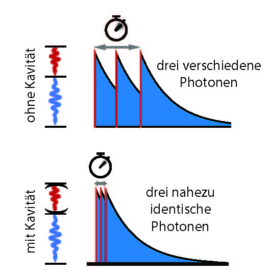
Illustration (University of Basel, Timon Baltisberger): Biexziton decay can generate photons of very high quality if the system is specifically controlled using an optical cavity. Under these conditions, 90 per cent of the photons are indistinguishable. Working in close collaboration, researchers from Paderborn University, the University of Basel and Ruhr University Bochum have made a significant breakthrough in the field of quantum communication. In their recently published paper in the...
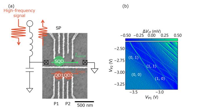
(a) The structure of the gate electrodes on the ZnO device used in the experiment in this paper. (b) The charge stability diagram indicating the formation of ZnO double quantum dot in few-electron regime. Researchers at Tohoku University, in collaboration with the National Institute for Materials Science (NIMS) and the University of Tokyo, have taken an important step toward semiconductor quantum computing using zinc oxide (ZnO). The team successfully demonstrated charge sensing,...
