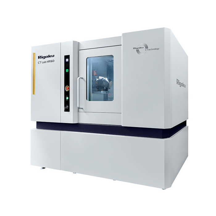
14 October 2026. Rigaku has launched the CT Lab HR160, an X-ray CT system that combines Rigaku's X-ray CT imaging expertise with Excillum's NanoTube N3 X-ray source. The system operates at up to 160 kV and achieves true 250 nm spatial resolution, a level Rigaku describes as industry-leading for CT systems in its class.
The resolution supports detailed, non-destructive 3D imaging of fine internal structures and defects that can be difficult to observe with conventional laboratory CT systems. Its cone-beam geometry allows users to adjust the field of view and resolution without changing the X-ray source or detector.
The system is designed for applications including solid-state batteries, semiconductor devices, multilayer ceramic capacitors (MLCCs), and power electronics, where internal inspection plays an increasingly important role in research, development, quality evaluation, and failure analysis.
Kiyoshi Ogata, General Manager of the Product Division at Rigaku, said: "CT Lab HR160 gives customers a new option for addressing increasingly complex analytical challenges in advanced materials and electronic devices."
Sara Haack, Chief Commercial Officer at Excillum AB, said: "We are pleased to see Excillum's X-ray source technology integrated into Rigaku's new CT Lab HR160 system."
Source: Rigaku news
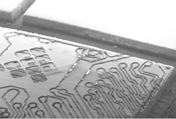
TESCAN ORSAY HOLDING, a.s. has described an A15 semiconductor failure analysis workflow that connects X-ray CT, ultrafast laser processing, optical and confocal microscopy, and SEM for progressive access to buried structures.
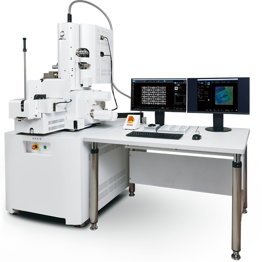
JEOL has started sales of HAXIS, a scanning electron microscope with low-angle argon ion milling and passive voltage contrast detection, for layer-by-layer semiconductor failure analysis.
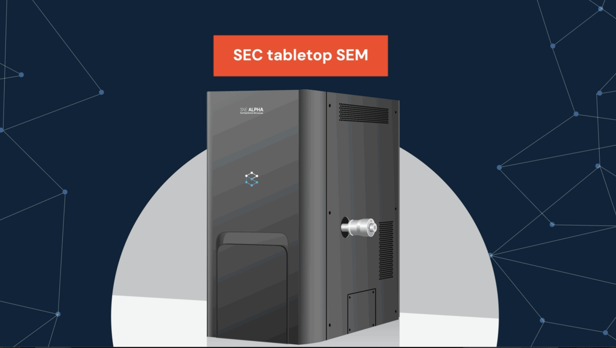
NanoImages, LLC has published details of its EBIC imaging technique for semiconductor failure analysis. The SNE-Alpha carries a factory EBIC port alongside its EDS, EBSD, Raman, and CL ports, with a 1-30 kV range.