University of Colorado (CU Boulder)
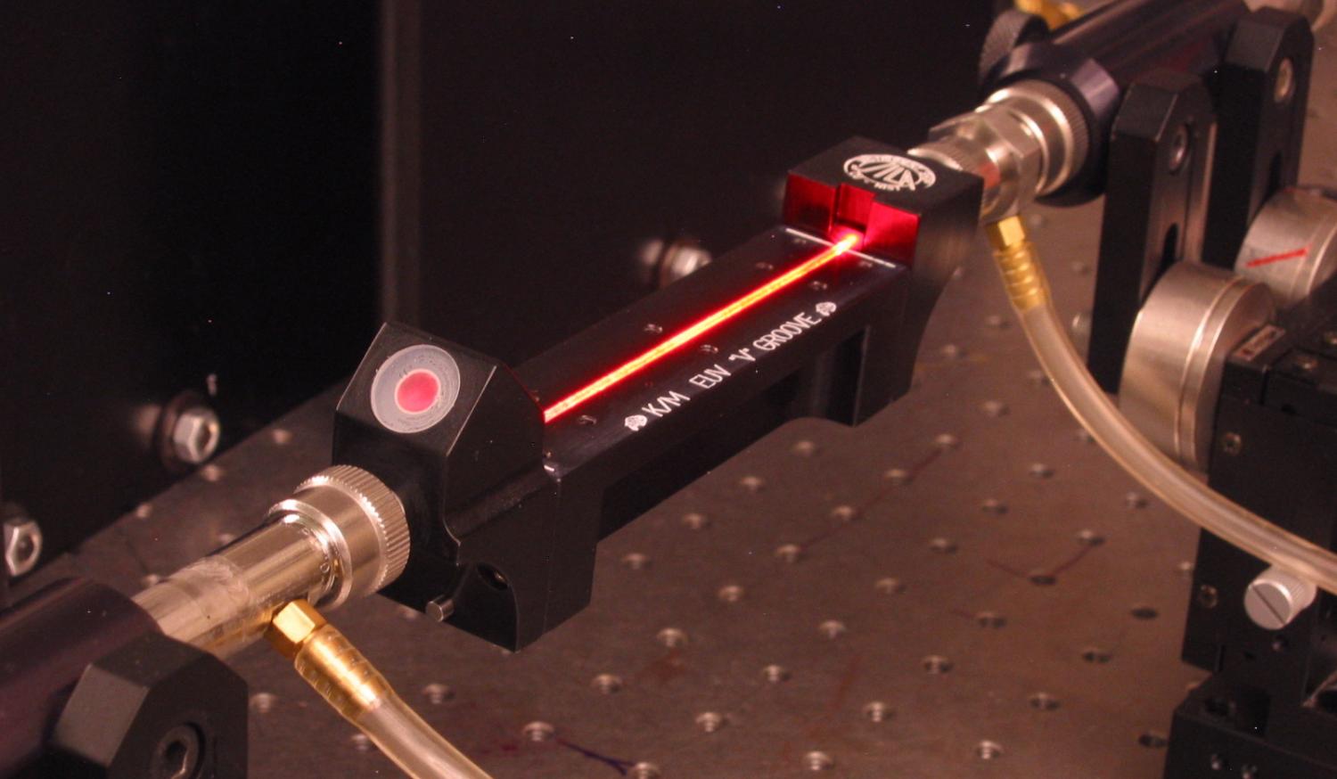
University of Colorado Boulder researchers have used ultra-fast extreme ultraviolet lasers to measure the properties of materials more than 100 times thinner than a human red blood cell.
The team, led by scientists at JILA, reported its new feat of wafer-thinness this week in the journal Physical Review Materials. The group's target, a film just 5 nanometers thick, is the thinnest material that researchers have ever been able to fully probe, said study coauthor Joshua Knobloch.
"This is a record-setting study to see how small we could go and how accurate we could be," said Knobloch, a graduate student at JILA, a partnership between CU Boulder and the National Institute of Standards and Technology (NIST).
He added that when things get small, the normal rules of engineering don't always apply. The group discovered, for example, that some materials seem to get a lot softer the thinner they become.
The researchers hope that their findings may one day help scientists to better navigate the often-unpredictable nanoworld, designing tinier and more efficient computer circuits, semiconductors and other technologies.
"If you're doing nanoengineering, you can't just treat your material like it's a normal big material," said Travis Frazer, lead author of the new paper and a former graduate student at JILA. "Because of the simple fact that it's small, it behaves like a different material."
"This surprising discovery--that very thin materials can be 10 times more flimsy than expected--is yet another example of how new tools can helps us to understand the nanoworld better," said Margaret Murnane, a coauthor of the new research, professor of physics at CU Boulder and JILA fellow.
Nano wiggles
The research comes at a time when many technology firms are trying to do just that: go small. Some companies are experimenting with ways to build efficient computer chips that layer thin films of material one on top of the other--like a filo pastry, but inside your laptop.
The problem with that approach, Frazer said, is that scientists have trouble predicting how those flakey layers will behave. They're just too delicate to measure in any meaningful way with the usual tools.
To help in that goal, he and his colleagues deployed extreme ultraviolet lasers, or beams of radiation that deliver shorter wavelengths than traditional lasers--wavelengths that are well-matched to the nanoworld. The researchers developed a set-up that allows them to bounce those beams off of layers of material just a few strands of DNA thick, tracking the different ways those films can vibrate.
"If you can measure how fast your material is wiggling, then you can figure out how stiff it is," Frazer said.
Atomic disruption
The method has also revealed just how much the properties of materials can change when you make them very, very small.
In the most recent study, for example, the researchers probed the relative strength of two films made out of silicon carbide: one about 46 nanometers thick, and the other just 5 nanometers thick. The team's ultraviolet laser delivered surprising results. The thinner film was about 10 times softer, or less rigid, than its thicker counterpart, something the researchers weren't expecting.
Frazer explained that, if you make a film too thin, you can cut into the atomic bonds that hold a material together--a bit like unraveling a frayed rope.
"The atoms at the top of the film have other atoms underneath them that they can hold onto," Frazer said. "But above them, the atoms don't have anything they can grab onto."
But not all materials will behave the same way, he added. The team also reran the same experiment on a second material that was nearly identical to the first with one big difference--this one had a lot more hydrogen atoms added in. Such a "doping" process can naturally disrupt the atomic bonds within a material, causing it to lose strength.
When the group tested that second, flimsier material using their lasers, they found something new: this material was just as strong when it was 44 nanometers thick as it was at a meager 11 nanometers thick.
Put differently, the additional hydrogen atoms had already weakened the material--a bit of extra shrinking couldn't do anymore damage.
In the end, the team says that its new ultraviolet laser tool gives scientists a window into a realm that was previously beyond the grasp of science.
"Now that people are building very, very small devices, they're asking how properties like thickness or shape can change how their materials behave," Knobloch said. "This gives us a new way of accessing information about nanoscale technology."
Full characterization of ultrathin 5-nm low-k dielectric bilayers: Influence of dopants and surfaces on the mechanical properties
Travis D. Frazer, Joshua L. Knobloch, Jorge N. Hernández-Charpak, Kathleen M. Hoogeboom-Pot, Damiano Nardi, Sadegh Yazdi, Weilun Chao, Erik H. Anderson, Marie K. Tripp, Sean W. King, Henry C. Kapteyn, Margaret M. Murnane, and Begoña Abad
Physical Review Materials 4, 073603 (13 July 2020)
DOI: 10.1103/PhysRevMaterials.4.073603
Contact information:
Travis Frazer
Graduate Student at JILA/CU Boulder
travis.frazer@colorado.edu
Phone: 303-492-2083
Joshua Knobloch
Graduate Student at JILA/CU Boulder
Joshua.Knobloch@colorado.edu
Phone: 303-492-7764
Margaret Murnane
Professor of physics at CU Boulder and JILA fellow
murnane@jila.colorado.edu
Phone: 303-492-7839
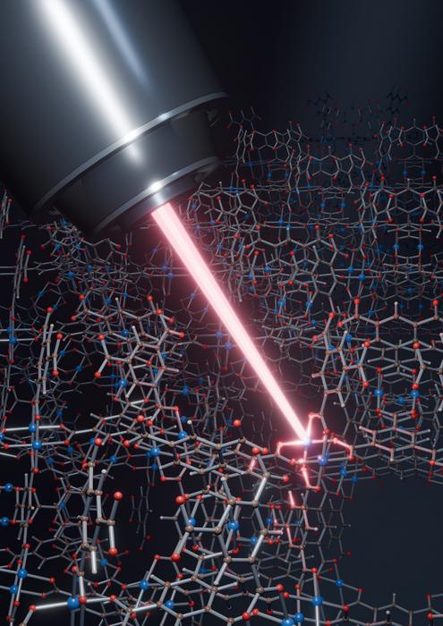
Filling the pores of a copper-based metal-organic framework with imidazolium ionic liquids makes the fragile material hard enough to pattern at room temperature. Treated Cu3BTC2 resisted the crystal damage seen in untreated samples during focused gallium ion beam etching, and researchers produced lines just 130 to 300 nanometres wide. The liquids appear to absorb heat and dissipate charge, and also raised hardness and thermal stability.
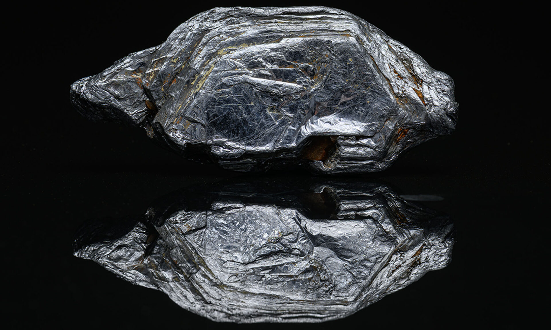
Engineers at the University of Rochester and Technion found that pressing a diamond nanoindenter tip a few nanometers into molybdenum can recrystallize the heat-resistant metal at room temperature, a process normally requiring about 1,000 degrees Celsius. Stopping the test just after the pop-in event reforms crystal grains in a tiny region around the dent, offering a way to repair defects and tailor properties locally.
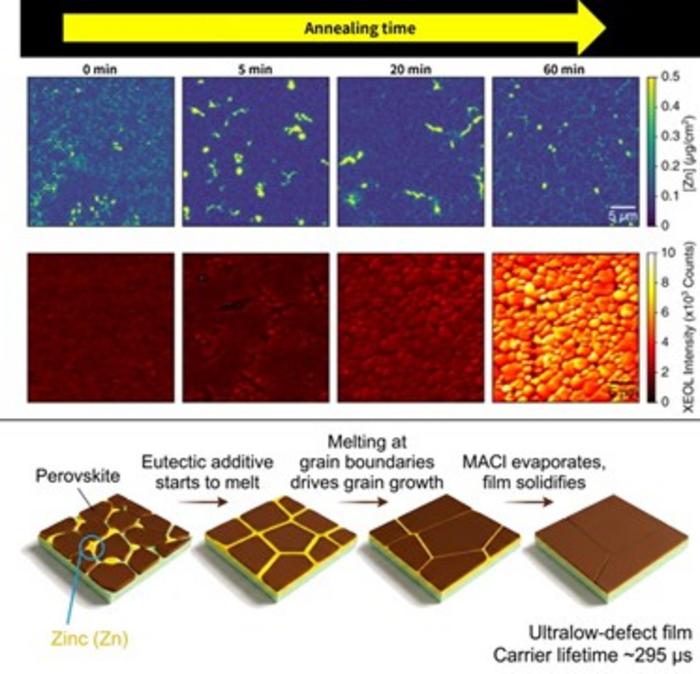
A eutectic mixture of methylammonium chloride and a zinc halide melts at about 100 degrees Celsius, forming a transient liquid layer at perovskite grain boundaries that lets crystals merge into larger, cleaner grains. The resulting films reached a carrier lifetime of roughly 295 microseconds and a surface recombination velocity of 0.3 cm/s, the lowest reported for lead halide perovskites.
This week in nanotech
9 deals tracked
New products
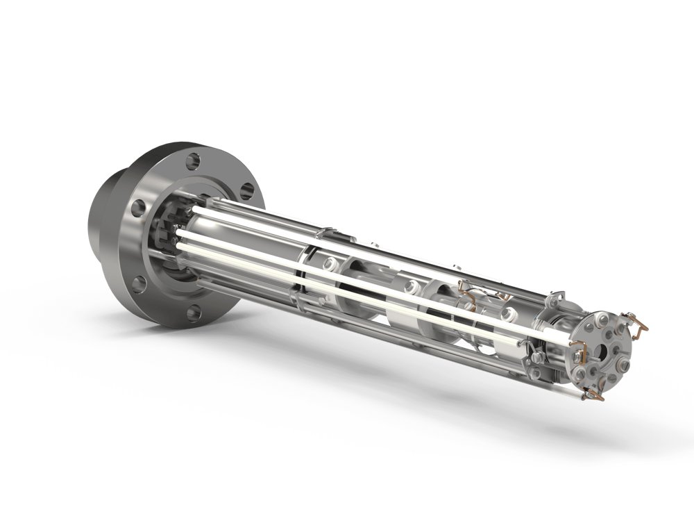 DLS-1 Mass Spectrometer for Fusion Gas AnalysisHiden Analytical Featured
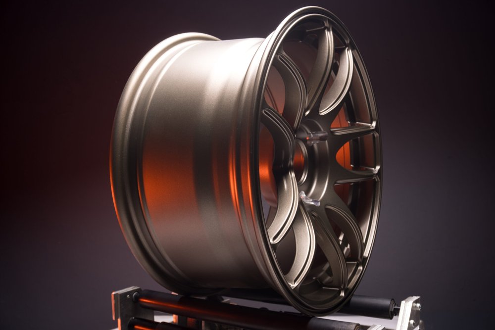 Ti-WCMBN Nanomaterialia Featured
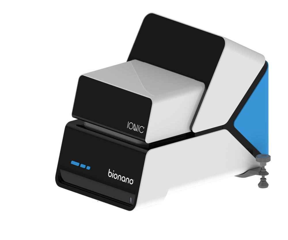 Ionic® Purification SystemBionano Genomics, Inc.
Market insights
Last 30 days: Semiconductors & Electronics was the busiest vertical: 39 of 130 events (30%).
Money raised per month