Sungkyunkwan University External Affairs Division (PR team)
A research team led by Professor Seong Sik Shin of the SKKU Advanced Institute of Nanotechnology (SAINT) at Sungkyunkwan University (SKKU), in international collaboration with the Korea Research Institute of Chemical Technology (KRICT), the University of California, San Diego, and Princeton University, has developed a next-generation perovskite semiconductor thin film with dramatically reduced defects. Using the same material platform, the researchers successfully demonstrated both high-performance solar cells and LEDs.
Perovskites have attracted considerable attention as key materials for next-generation electronic devices because of their low manufacturing costs and relatively simple processing. They can be used in solar cells that convert light into electricity as well as LEDs that convert electricity into light. However, when a liquid precursor solution is solidified into a thin film, microscopic crystal grains form and join together, often creating numerous defects at grain boundaries and surfaces. These defects can trap or eliminate photo-generated charge carriers, significantly reducing device performance and operational lifetime.
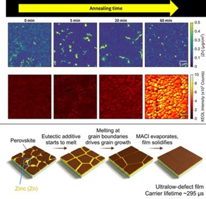
The research team found a solution in the eutectic phenomenon, in which the melting temperature of a mixture becomes substantially lower than that of its individual components. The researchers focused on the fact that when two materials with relatively high individual melting temperatures—methylammonium chloride (MACl) and a zinc halide (ZnX₂)—are combined, the mixture begins to melt at a much lower temperature.
When the perovskite film was gently heated to around 100°C, the mixture located at the grain boundaries transformed into a thin liquid layer. In the liquid state, atoms can diffuse approximately 10,000 times faster than in a solid, allowing small crystal grains to rapidly merge and grow into larger, cleaner crystals with fewer defects. MACl, which facilitates crystal growth, subsequently evaporates during thermal annealing, while the remaining zinc segregates toward the grain boundaries and helps suppress defects.
The resulting films demonstrated the highest level of quality reported to date for perovskite thin films. The charge-carrier lifetime reached approximately 295 μs, among the longest ever reported, while the surface recombination velocity, which indicates carrier losses caused by surface defects, was reduced to 0.3 cm/s, the lowest reported value for lead halide perovskites. This performance is comparable to the best values reported for passivated silicon.
Solar cells fabricated using the new films achieved a high power conversion efficiency of 26.5% (certified 25.9%), together with an open-circuit voltage of 1.208 V, a certified record for solar cells with the same n-i-p architecture. Remarkably, an LED with the same device architecture as the solar cell achieved an external quantum efficiency of 26.1%, demonstrating that a single device structure can function both as a power-generating device that absorbs light and as a light-emitting device.
Dr. Seongsik Nam, co-first author of the study, said, “We reduced the surface recombination velocity to 0.3 cm/s, the lowest reported for perovskite thin films, demonstrating that solution processing can achieve surface quality comparable to that of silicon. As we have also demonstrated strong performance over large areas, we expect this technology to help accelerate the commercialization of perovskite solar cells.”
Professor Seong Sik Shin, who led the research, said, “This study is the world’s first to develop a crystal-growth method based on a volatile eutectic mixture that fundamentally reduces defects in perovskites. Beyond realizing both a highly efficient solar cell and an LED within a single device architecture, the process requires no expensive specialized equipment.”
He added, “We expect this approach to find broad applications not only in various optoelectronic devices, including displays and photodetectors, but also across the wider field of materials science.”
The study was jointly led by corresponding authors Professor Seong Sik Shin of Sungkyunkwan University, Professor David P. Fenning of the University of California, San Diego, and Professor Dane W. deQuilettes of Princeton University. Dr. Seongsik Nam of Sungkyunkwan University, Dr. Jason J. Yoo of the Korea Research Institute of Chemical Technology, and Dr. Connor J. Dolan of the University of California, San Diego participated as co-first authors.
Reference
Volatile eutectics to tailor crystallization for perovskite optoelectronics
Jason J. Yoo, Connor J. Dolan, Seongsik Nam, Jinho Lee, Kyu Min Kang, Bong Joo Kang, Rushik Desai, Niranjana Mohan Kumar, Arkita Chakrabarti, Daesoo Kim, Jang Hee Cho, Donghyuk Chung, Jack R. Palmer, Kelly X. Vences, Zhewen J. D. Deng, Yanqi Luo, Barry Lai, Tao Zhou, Zhonghou Cai, Martin V. Holt, Andrew M. Kiss, In Sun Cho, Dong Hyun Kim, Jun Hong Noh, Mariana I. Bertoni, Arun Mannodi-Kanakkithodi, Dane W. deQuilettes, David P. Fenning, and Seong Sik Shin
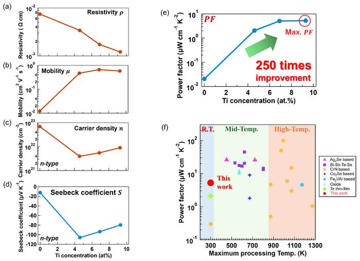
Researchers at Tohoku University have raised the power factor of chromium nitride thin films 250-fold by doping them with small amounts of titanium, reaching 5.26 µW cm⁻¹ K⁻². Titanium's stronger affinity for nitrogen suppresses nitrogen vacancies, cutting carrier concentration while boosting electron mobility by roughly two orders of magnitude.

Noak, a spin-off of imec and Hasselt University, has secured €5 million in seed funding to industrialize perovskite-silicon tandem solar cells, which promise conversion efficiencies of 30 to 35 percent compared with the roughly 27 percent practical limit of conventional silicon. The technology rests on proprietary perovskite layer stacks and scalable deposition methods, backed by five years of outdoor testing at more than ten sites across three continents.
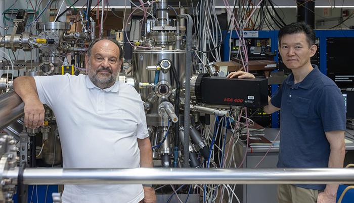
Researchers used terahertz light to probe magnetic vortices inside iron-based superconductors, separating two groups of trapped particles by their response to left and right-handed light polarization. Comparing films with different selenium content showed similar superconducting temperatures can hide very different internal behavior. The technique, demonstrated on ultrathin films, offers a new way to screen materials for magnets and other applications where vortices cause energy losses.
This week in nanotech
$13.6M raised
3 funding rounds · 20 deals tracked
New products
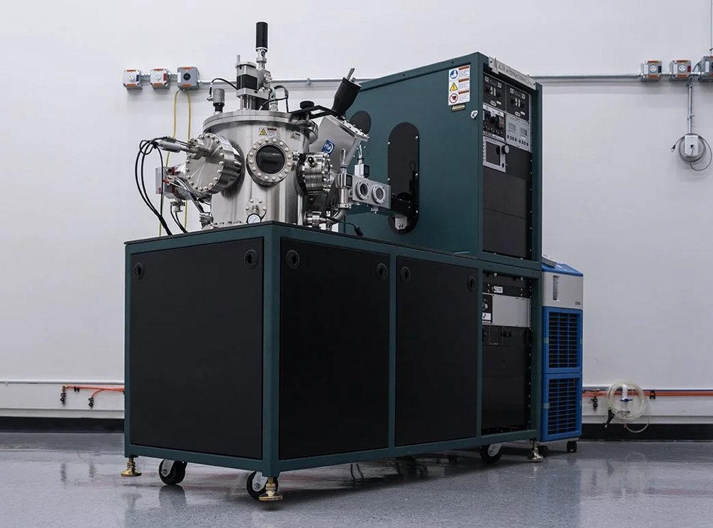 Orion Sputtering Deposition SystemsAJA International Featured
 Ti-WCMBN Nanomaterialia Featured
 NanoFlow® S1-20Levidian
Market insights
Last 30 days: Quantum Technologies was the busiest vertical: 61 of 192 events (32%).
Money raised per month