Swansea University
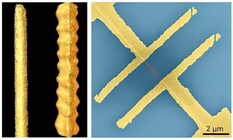
The crystal structure at the surface of semiconductor materials can make them behave like metals and even like superconductors, a joint Swansea/Rostock research team has shown. The discovery potentially opens the door to advances like more energy-efficient electronic devices.
Semiconductors are the active parts of transistors, integrated circuits, sensors, and LEDs. These materials, mostly based on silicon, are at the heart of today's electronics industry.
We use their products almost continuously, in modern TV sets, in computers, as illumination elements, and of course as mobile phones.
Metals, on the other hand, wire the active electronic components and are the framework for the devices.
The research team, led by Professor Christian Klinke of Swansea University's chemistry department and the University of Rostock in Germany, analysed the crystals at the surface of semiconductor materials.
Applying a method called colloidal synthesis to lead sulphide nanowires, the team showed that the lead and sulphur atoms making up the crystals could be arranged in different ways. Crucially, they saw that this affected the material's properties.
In most configurations the two types of atoms are mixed and the whole structure shows semiconducting behaviour as expected.
However, the team found that one particular "cut" through the crystal, with the so called {111} facets on the surface, which contains only lead atoms, shows metallic character.
This means that the nanowires carry much higher currents, their transistor behaviour is suppressed, they do not respond to illumination, as semiconductors would, and they show inverse temperature dependency, typical for metals.
Dr. Mehdi Ramin, one of the researchers from the Swansea/Rostock team, said:
"After we discovered that we can synthesize lead sulphide nanowires with different facets, which makes them look like straight or zigzag wires, we thought that this must have interesting consequences for their electronic properties.
But these two behaviours were quite a surprise to us. Thus, we started to investigate the consequences of the shape in more detail."
The team then made a second discovery: at low temperatures the skin of the nanostructures even behaves like a superconductor. This means that the electrons are transported through the structures with significantly lower resistance.
Professor Christian Klinke of Swansea University and Rostock University, who led the research, said:
"This behaviour is astonishing and certainly needs to be further studied in much more detail.
But it already gives new exciting insights into how the same material can possess different fundamental physical properties depending on its structure and what might be possible in the future.
One potential application is lossless energy transport, which means that no energy is wasted.
Through further optimization and transfer of the principle to other materials, significant advances can be made, which might lead to new efficient electronic devices.
The results presented in the article are merely a first step in what will surely be a long and fruitful journey towards new thrilling chemistry and physics of materials."
Function Follows Form: From Semiconducting to Metallic toward Superconducting PbS Nanowires by Faceting the Crystal
Mohammad Mehdi Ramin Moayed, Sascha Kull, Angelique Rieckmann, Philip Beck, Michael Wagstaffe, Heshmat Noei, Andreas Kornowski, Ana B. Hungria, Rostyslav Lesyuk, Andreas Stierle, Christian Klinke
Advanced Materials (2020)
Contact information:
Christian Klinke
Associate Professor of Chemistry at Swansea University & Rostock University
christian.klinke@swansea.ac.uk
Phone: +44 1792 604278
Nanostructures and nanomaterials group

Waste polyamide-derived CQDs show continuous photoluminescence tuning from 308 to 552 nm through sequential defect-state engineering, with optical transition energies decreasing from 4.32 to 2.50 eV. @Christian Ebere Enyoh from Saitama University Carbon quantum dots (CQDs) are fluorescent carbon nanomaterials with potential applications in sensing, optoelectronics, displays, anti-counterfeiting, and environmental technologies. Their optical properties can be adjusted by modifying the carbon...

The researchers used circularly polarized light at normal incidence and found that helicity-dependent photocurrents appeared perpendicular to the crystal’s polarization but vanished when measured parallel to it, supporting a bulk origin of CPGE. @Institute of Science Tokyo The circular photogalvanic effect (CPGE), a phenomenon that generates helicity-dependent photocurrents in noncentrosymmetric materials, can originate purely from a crystal's internal structure without contribution from the...

Summary of gold nanoparticle growth programming in liposome based on localization of biomineralization peptide The position of biomineralization peptides within liposomes can influence how gold nanoparticles grow, reports a research team from Institute of Science Tokyo. Peptides localized at the membrane interface promote branched structures, while those confined to the liposome interior favor spherical nanoparticles. The findings offer a new strategy for controlling nanoscale reaction...
