Leuven, 10 November 2026. Vertical Compute has announced an expanded partnership with imec to accelerate the commercial deployment of its vertically integrated memory (VIM) technology. The two organisations are moving beyond an initial R&D service agreement to operate in an integrated engineering model, with the aim of bringing the memory architecture to market.
The collaboration covers complete validation of Vertical Compute's test chip in 40nm and prepares manufacturing of its first pre-production product in 16nm. The 16nm chip will be manufactured at a commercial foundry, with the proprietary VIM layer added directly at imec. The work will use imec's NanoIC pilot line, an EU-funded initiative intended to bridge advanced semiconductor research and industrial production.
Vertical Compute's technology stacks high-density magnetic memory directly above compute logic. According to the company, this reduces the path between data and compute from centimeters to tens of nanometers within a single manufacturing flow, so data is stored and accessed locally where computation happens.
"The defining limit on AI scaling today isn't processing power, it's the exponential cost and energy of moving data" said Sylvain Dubois, co-founder and CEO of Vertical Compute. "Taking our Vertically Integrated Memory from a breakthrough concept to 16nm production requires world-class ecosystem alignment."
"The acceleration of AI demands paradigm-level innovation at the hardware level," added Sri Samavedam, imec senior VP. "Vertical Compute's approach to vertically integrated memory is exactly the kind of architectural shift the industry needs."
The NanoIC pilot line's acquisition and operation are jointly funded by the Chips Joint Undertaking, through the European Union's Digital Europe (101183266) and Horizon Europe programmes (101183277), and by the participating states Belgium (Flanders), France, Germany, Finland, Ireland and Romania.
Source: Vertical Compute news
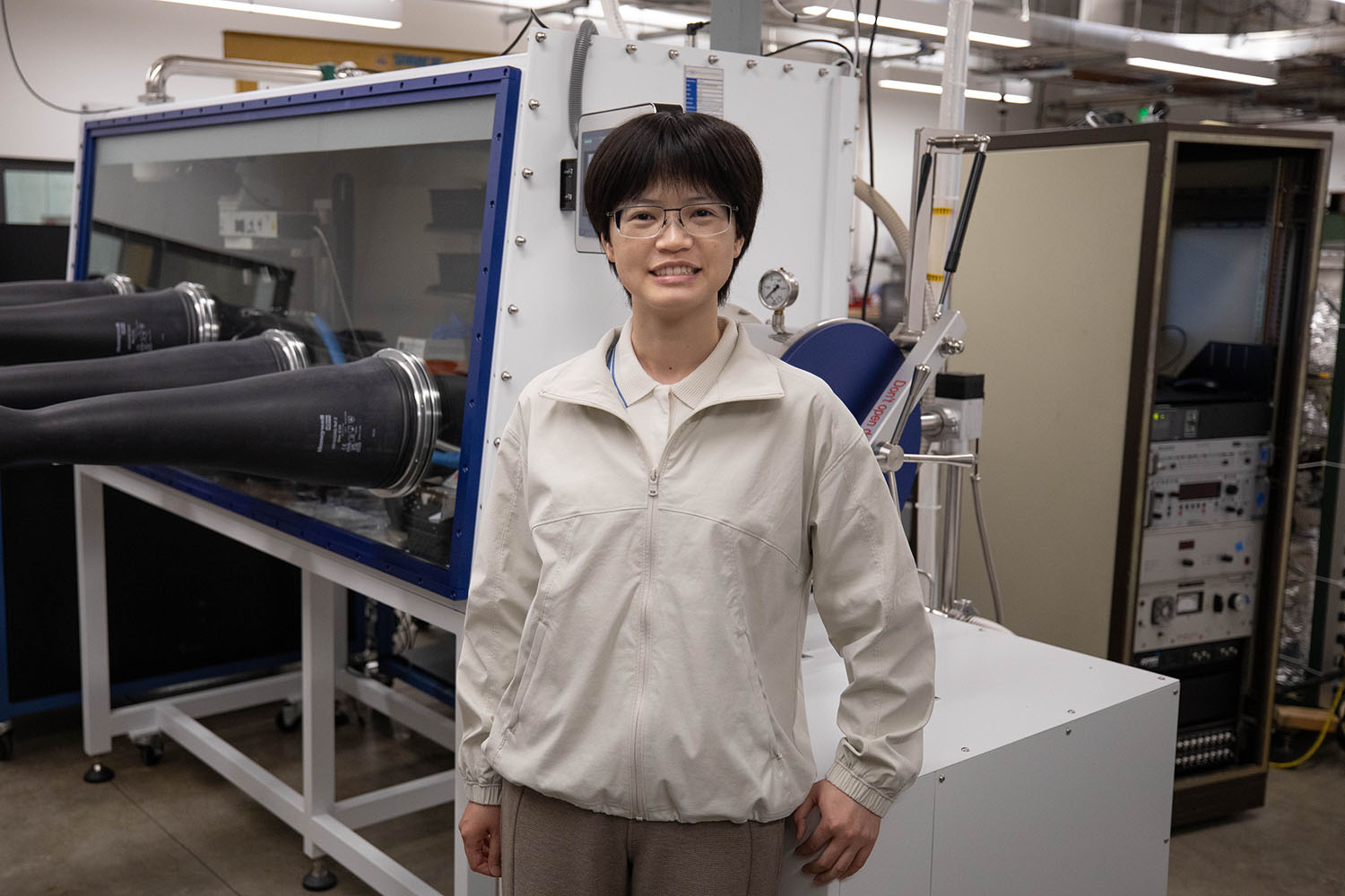
Researchers have identified a chiral superlattice in uranium oxytelluride, a material known since the 1960s but largely overlooked. Using transmission electron microscopy and scanning tunneling microscopy, the team observed a twisted atomic pattern whose handedness shapes electron behavior. The crystal combines ferromagnetic and antiferromagnetic traits in one compound, a rare pairing that could inform faster, more robust magnetic memory devices.
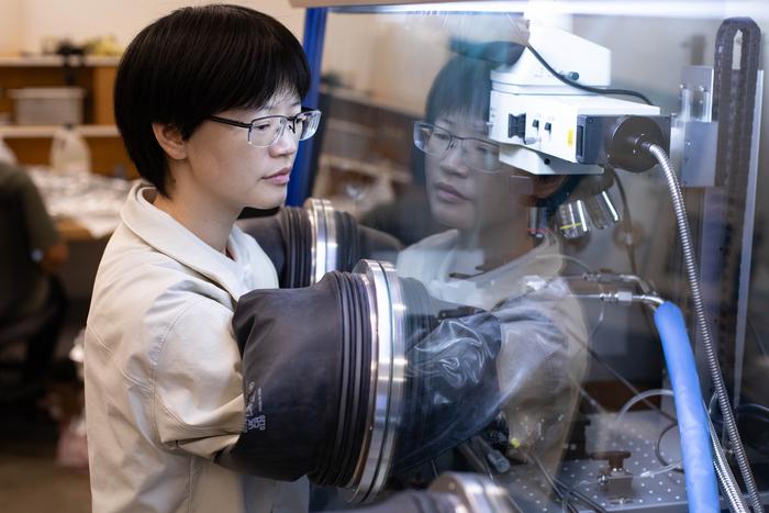
Microscopy of uranium oxytelluride has revealed a chiral superlattice, a twisted atomic pattern that was previously unrecognized in a compound known since the 1960s. Electrons moving through the spiral structure behave unexpectedly because the material combines ferromagnetic and antiferromagnetic order, an unusual pairing that could support faster, more robust magnetic memory.
AlixLabs AB has started a six-month evaluation project to assess its APS™ technology for advanced semiconductor patterning within the NanoIC pilot line, coordinated by imec.
This week in nanotech
$109M raised
3 funding rounds · 18 deals tracked
New products
 Ti-WCMBN Nanomaterialia Featured
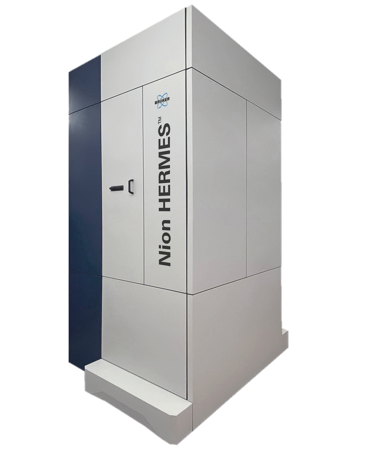 Nion-compatible In Situ STEM Holders for Electrical BiasingHummingbird Scientific Featured
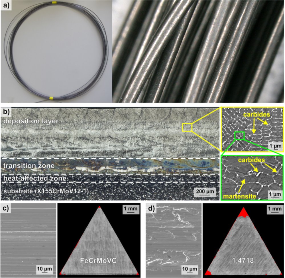 Fe85Cr4Mo8V2C1 wire filler materialLeibniz Institute for Solid State and Materials Research Dresden - IFW Dresden
Market insights
Last 30 days: Semiconductors & Electronics drew the most money: $545M.
Money raised per month