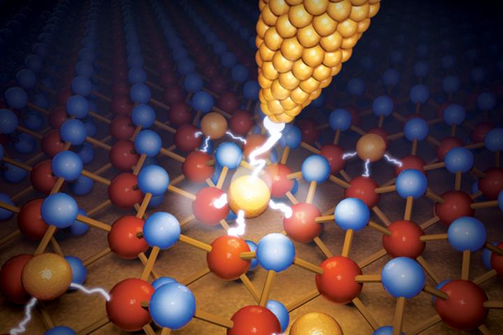
Faster, smaller, smarter and more energy-efficient chips for everything from consumer electronics to big data to brain-inspired computing could soon be on the way after engineers at The University of Texas at Austin created the smallest memory device yet. And in the process, they figured out the physics dynamic that unlocks dense memory storage capabilities for these tiny devices.
The research published recently in Nature Nanotechnology builds on a discovery from two years ago, when the researchers created what was then the thinnest memory storage device. In this new work, the researchers reduced the size even further, shrinking the cross section area down to just a single square nanometer.
Getting a handle on the physics that pack dense memory storage capability into these devices enabled the ability to make them much smaller. Defects, or holes in the material, provide the key to unlocking the high-density memory storage capability.
"When a single additional metal atom goes into that nanoscale hole and fills it, it confers some of its conductivity into the material, and this leads to a change or memory effect," said Deji Akinwande, professor in the Department of Electrical and Computer Engineering.
Though they used molybdenum disulfide - also known as MoS2 - as the primary nanomaterial in their study, the researchers think the discovery could apply to hundreds of related atomically thin materials.
The race to make smaller chips and components is all about power and convenience. With smaller processors, you can make more compact computers and phones. But shrinking down chips also decreases their energy demands and increases capacity, which means faster, smarter devices that take less power to operate.
"The results obtained in this work pave the way for developing future generation applications that are of interest to the Department of Defense, such as ultra-dense storage, neuromorphic computing systems, radio-frequency communication systems and more," said Pani Varanasi, program manager for the U.S. Army Research Office, which funded the research.
The original device - dubbed "atomristor" by the research team - was at the time the thinnest memory storage device ever recorded, with a single atomic layer of thickness. But shrinking a memory device is not just about making it thinner but also building it with a smaller cross-sectional area.
"The scientific holy grail for scaling is going down to a level where a single atom controls the memory function, and this is what we accomplished in the new study," Akinwande said.
Akinwande's device falls under the category of memristors, a popular area of memory research, centered around electrical components with the ability to modify resistance between its two terminals without a need for a third terminal in the middle known as the gate. That means they can be smaller than today's memory devices and boast more storage capacity.
This version of the memristor - developed using the advanced facilities at the Oak Ridge National Laboratory - promises capacity of about 25 terabits per square centimeter. That is 100 times higher memory density per layer compared with commercially available flash memory devices.
Contact
Deji Akinwande
Electrical and Computer Engineering
The University of Texas at Austin
deji@ece.utexas.edu
Reference
Observation of single-defect memristor in an MoS2atomic sheet
Saban M. Hus, Ruijing Ge, Po-An Chen, Liangbo Liang, Gavin E. Donnelly, Wonhee Ko, Fumin Huang, Meng-Hsueh Chiang, An-Ping Li & Deji Akinwande

Researchers at the University of Basel have identified and coherently controlled so called forbidden vibrational transitions in individual trapped nitrogen molecular ions without destroying them. Using quantum logic spectroscopy, a single calcium ion served as messenger, letting the team probe the molecule repeatedly and determine its fundamental vibrational frequency ten times more precisely than before.
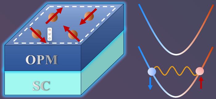
Odd-parity magnets host an intrinsic hidden Zeeman field that lifts Kramers degeneracy without any applied field, researchers report. Using an f-wave magnet model on a triangular lattice, the team shows how non-relativistic spin splitting and this hidden field combine to stabilize s-wave superconductivity far beyond the Pauli limit.

Rhombohedral hexalayer graphene, in which six carbon sheets are stacked with a slight lateral offset like staircase steps, hosts both superconductivity and electrically controllable orbital magnetism, researchers report in Nature Physics. The arrangement yields a rich collection of quantum states in a simple carbon-based material, positioning rhombohedral multilayer graphene as a platform for probing the fundamental mechanisms of superconductivity and magnetism and potentially for new ways of…
This week in nanotech
9 deals tracked
New products
 Orion Sputtering Deposition SystemsAJA International Featured
 Ti-WCMBN Nanomaterialia Featured
 Hold Down & Release Mechanisms (HDRM) REACT – 5KN, 15KN and 35KN space qualified resettable mechanismsARQUIMEA
Market insights
Last 30 days: Semiconductors & Electronics was the busiest vertical: 39 of 130 events (30%).
Money raised per month