By JC Nabity Lithography Systems
NPGS is the lowest cost high performance lithography system for SEM/STEM/FIB microscopes that is available. An SEM lithography system is a tool which can be used in a wide variety of applications. The basic lithography process allows patterns to be defined on a flat surface. The subsequent processing, such as metal evaporation or etching, will determine the final structure. NPGS is unique in that it provides a very flexible system which is ideally suited to the wide range of activities in basic research and R&D activities. Examples of some of the structures made with NPGS include: single electron devices, quantum chaos devices, quantum dots, tunnel junctions, one and two dimensional metal wires/films, linear/circular gratings, surface acoustic wave (SAW) devices, split gate devices, as well as "larger" structures such as micromechanical devices, waveguides, and bonding pads. Since NPGS is so versatile, it is well suited for use in almost any application that can be done with e-beam lithography. The primary exceptions are structures covering large areas which require the capabilities of a multi-million dollar beam writer. However, in some cases, the many advanced features of NPGS allow it to be used to fabricate structures that are more difficult to make on an expensive beam writer. NPGS can also be used for lithography with a Focused Ion Beam (FIB) system. In fact, a single NPGS installation can be configured with a dual mode to control either the electron beam or the ion beam on dual FIB/SEM systems, including the Nova Nanolab and Helios models from FEI and the Crossbeam and Auriga models from Zeiss. The NPGS License agreement gives the original buyer full rights to use the "Microscope Installation" of the NPGS software without any time limitations, as long as it is only installed on a single PC. The PC with the "Microscope Installation" (which contains the NPGS hardware) may be moved between different microscopes (which may require different sets of cables/connections) or may be connected simultaneously to two microscopes if they are near each other (with the NPGS Output Relay Box, which allows use of one microscope or the other for lithography). Having simultaneous connections is especially useful for dual beam ion/electron microscopes. The NPGS License agreement allows unlimited "Office Installations" of the NPGS software which may be used within the university or organization where NPGS is installed. The "Office Installation" allows full pattern and run file design/edit/simulation capabilities, but has no pattern writing capabilities, since no NPGS hardware is used. NPGS also ships with a site license of QCAD Professional which is used for pattern design within NPGS. For universities, the QCAD site license allows unlimited installations. For other organizations, it allows 20 installations. Having multiple "Office Installations" of NPGS and QCAD make it easy for each NPGS user to do pattern design away from the microscope. The ultimate writing resolution depends on the SEM in use, the resist, and the operator's skill at optimizing the SEM. With NPGS, features of 20 nm and less are routinely written when using a thermal FE SEM, 30 nm and less when using a 40 kV conventional SEM, and even smaller when using a high voltage STEM. NPGS uses a true vector writing mode which gives the user the maximum control over the beam. For example, the beam will move along sloped lines and tangent to arcs and circles. Also, when filling arbitrary polygons, the beam will sweep parallel to one side of the polygon as specified by the user. This approach enhances the exposure quality over systems using a simple xy raster method or one that breaks each arbitrary polygon into trapezoids with different scan directions. In addition to the vector writing mode, NPGS also provides a raster mode for writing bitmaps which can be useful for FIB milling. NPGS only runs on a PC running the Windows operating system, however, pattern files can be created on other systems and transferred to NPGS to be written.
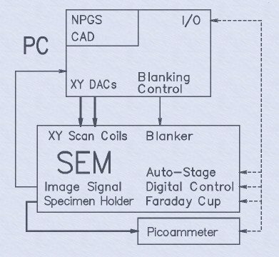
System Description: Software: NPGS - Version 9.2 (site-license included; see "Upgrade History" for a listing of the most advanced features.) QCAD Professional v3.32 (site-license included; unlimited use for educational institutions). 64 bit Windows 11 Pro (when PC is included). Hardware: 16-bit High speed PCIe516 lithography board. Cables to connect NPGS to microscope. Optional relay adapter to share microscope input with another accessory, typically an EDX system. Workstation PC with (or better): 8 GB RAM, 500 Gb Hard Disk, DVDRW Drive. 24" LCD Monitor. LAN, USB, Serial Port. NPGS Installation Guide: Detailed installation instructions for nearly every microscope. How to calibrate absolute pattern size and aspect ratio. Checklist for testing and characterizing the microscope. Interface instructions for serial or Ethernet microscope interface, as appropriate. NPGS User's Manual including: Detailed instructions for NPGS software. Detailed tutorial on how to set up and run a Scanning Electron Microscope for writing nanometer patterns. Sample patterns and run parameters. Solutions to Problems section covering nearly all common microscope and/or lithography problems. NPGS Training: Optional on-site user training. The user must supply: SEM, STEM, FIB, HIM (Helium Ion Microscope), or dual SEM/FIB with: XY External Scan Control Input (within +/- 3 to +/- 10 volts, 2k ohms). Image Signal Output (within +/- 10 volts). Picoammeter for Measuring Beam Current (0.1 pA resolution or better; typically Keithley 6485). A dual SEM/FIB can have both beams controlled by NPGS, but only one at a time where either a software or hardware switch (depending on microscope model) will select the writing mode. Recommended: Beam Blanker with rise/fall times <1 usec (digital input within +/- 5 v and <200 mA). (Slow Beam Shutter or no blanker will also work). Fine Z stage control to ~1um. Faraday Cup (apertures to make cup are included with NPGS). Scan Rotation Option. Gold on Carbon SEM standard mounted on sample holder. Stray AC less than 3x10⁻⁷ Tesla(p-p); Magnetic shielding for chamber or active field cancelling system can reduce interference. Vibration less than 2x10⁻⁶ meters(p-p) over 5 Hz. Other Configurations: (NPGS Software is Identical to Full System) The user may supply any of the following: Workstation PC. Installation. Minimum computer requirements for NPGS v9 and higher: 2 GHz CPU recommended. Windows XP (32 or 64 bit Win7/10/11 Pro recommended). 256 MB RAM (4 GB or more recommended). CD ROM. 1 available PCIe Slot (for full length board, 12.3" = 31.2 cm). 1280x1024 Graphics. Serial Ports and/or Ethernet interface may be required for optional control of a stage and/or SEM. NPGS Updates: NPGS software updates are available at no charge to current NPGS users.
CATEGORY
Software: - NPGS - Version 9.2 (site-license included) - QCAD Professional v3.32 (site-license included; unlimited use for educational institutions). - 64 bit Windows 11 Pro (when PC is included). Hardware: - 16-bit High speed PCIe516 lithography board. - Cables to connect NPGS to microscope. - Optional relay adapter to share microscope input with another accessory, typically an EDX system. - Workstation PC with (or better): - 8 GB RAM, 500 Gb Hard Disk, DVDRW Drive. - 24" LCD Monitor. - LAN, USB, Serial Port. NPGS Installation Guide: - Detailed installation instructions for nearly every microscope. - How to calibrate absolute pattern size and aspect ratio. - Checklist for testing and characterizing the microscope. - Interface instructions for serial or Ethernet microscope interface, as appropriate. NPGS User's Manual including: - Detailed instructions for NPGS software. - Detailed tutorial on how to set up and run a Scanning Electron Microscope for writing nanometer patterns. - Sample patterns and run parameters. - Solutions to Problems section covering nearly all common microscope and/or lithography problems.
CATEGORY
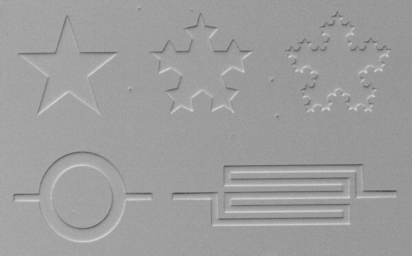
This image shows the powerful capability of the NPGS "Filled Polygon" feature. Each of these structures was created in the DesignCAD program as a single polygon, and they are automatically filled by NPGS during the pattern writing. The patterns were written in 950k PMMA and are shown after development and Au sputtering, but with no liftoff. The scale on this image is indicated by the serpentine structure which has a linewidth of 1 micron. The two stars on the right were created using a "fractal" program that runs within DesignCAD. These "fractal" stars show both the complexity allowed in a filled polygon (any shape with up to 1000 vertices in NPGS v9) and the power of the programming environment within DesignCAD. The circular structure is a polygon with 122 vertices which are so close together that the short straight lines defining the inner and outer circles are not observable. (This image was acquired with the NPGS Digital Imaging Feature.)
CATEGORY
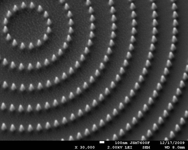
This is an SEM image of platinum features deposited directly onto a substrate using Electron Beam Induced Deposition (EBID). The features were written using NPGS with a thermal FE SEM with an OmniGIS Gas Injection System attached. The precursor used to deposit these platinum (Pt) features was MeCpPtMe3 [Trimethyl(methylcyclopentadienyl)platinum(IV)]. These features were written at 30 kV with 1 nA of beam current. The writing time for the features in the image was approximately 2 minutes. Note how the base of the features are ~100 nm in diameter, while the tips are much smaller. NPGS can also be used with ion beam microscopes which have a gas injection system to perform ion beam induced deposition.
CATEGORY
