By Aixtron Se
The BM (Black Magic) range of systems is a turnkey solution for the production of graphene, carbon nanotubes, nanofibers and nanowires. These innovative systems are based upon thermal CVD and plasma enhanced processes. The materials produced by our BM systems can be used in a variety of applications including transistors, interconnects, flexible electronics, energy storage, thermal management, sensors and filters.
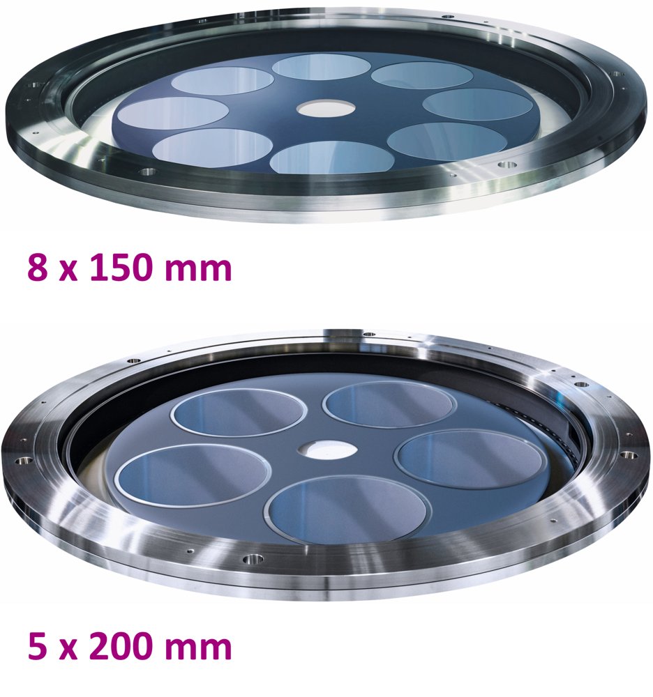
150/200 mm high throughput epitaxy for GaN power & RF applications . Our product for 150/200 mm GaN epitaxy G10-GaN - Highest wafer/m² fab area 3 process chamber compact cluster design with 50 % footprint reduction - Best in class device yield 3x on-wafer uniformity improvement at lowest particle level for all wafers (within run, run-to-run, chamber-to-chamber) - Lowest epi cost/wafer in the market 25% lower epi cost than any other platform Planetary Reactor® Your benefits - Highest wafer yield Low particle density (~0.1/cm²) Excellent uniformity (on-wafer, wafer-to-wafer) - Best in class productivity Outstanding reproducibility ≥90 % equipment uptime - Best in class epi cost Highest throughput/m² fab Lowest labor & chemical cost Our solutions - Fully automated wafer handling (C2C) - Novel wafer carrier design - Individual wafer close loop topside temp. control - Individual control of thickness & composition uniformity by 5-flow injector - Automated chamber cleaning - Long lifetime consumables - Smart system with predictive functionalities - Advanced chamber-to-chamber matching capabilities - Large capacity batch Planetary Reactor® - Compact cluster design with 3 process chambers - Highest chemical efficiency by 5-flow injector - Lowest operator assistance due to 50 wafer capacity on C2C The best of both worlds Single wafer performance at lowest batch processing cost Composition uniformity On-wafer device uniformity (650V application) G10-GaN enables seamless process transfer from today's tool of record AIX G5+ C - Same cassette-to-cassette wafer handling - „On-board“ calibration and control modes for process matching - Identical process chamber size and wafer configuration High productivity MOCVD solution for 150/200 mm GaN power & RF applications
CATEGORY
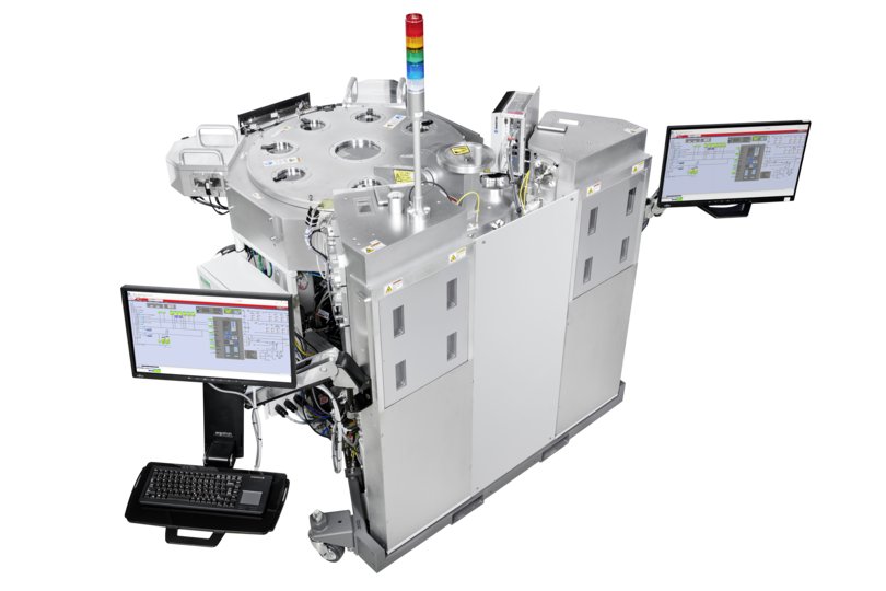
The Enabling MOCVD Solution Fully Automated MOCVD for High Volume Production of GaAs/InP Materials Cassette-to-Cassette Wafer Handling - Fully automated loading of wafers - Compatible with current and future wafer sizes 75 mm | 100 mm | 150 mm | 200 mm | optional SMIF port - Vacuum cassette elevators for 2 x 25 wafer cassettes - Clean environment for lowest defect levels - Significant reduction of labor cost – both on operator and expert level Fully Automated MOCVD for High Volume Production of GaAs/InP Materials Market Opportunity - Future proof - Compatible with current and future wafer sizes 75 mm | 100 mm | 150 mm | 200 mm | optional SMIF port - Highest uniformity and repeatability – throughout production campaigns - Best particle performance in the market at lowest operational cost per good wafer Planetary Reactor® Your benefits - Reduced labor cost, eliminate night shift - Up to 10X lower particles, down to 0.1/cm² - Unsurpassed reproducibility - Exceptionally long campaigns - Best in class yields - Highest quality epitaxial layers - Best Cost of Ownership - Highest throughput of its class Our solutions - Fully automated processes with Cassette-to-Cassette handling - Automated chamber etch back - Planetary technology with single wafer performance - Wafer-level control of uniformity and temperature by numerous chamber design innovations - Largest capacity batch reactor platform for maximized Fab output - Unmatched chemical efficiency by novel reactor design innovations Addressing the tightened requirements of future markets Best in class single wafer performance – throughout production campaign Wavelength uniformity for Micro LEDs F-P Dip uniformity for VCSEL
CATEGORY
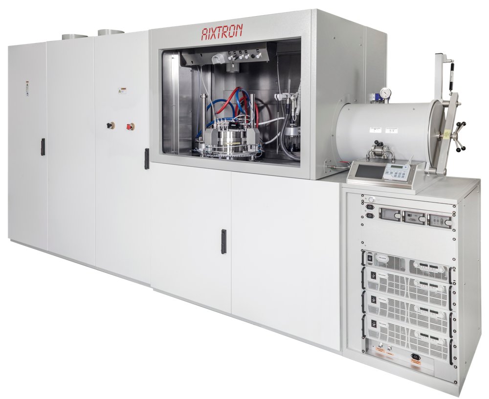
DEPOSITION SYSTEM FOR COMPOUND SEMICONDUCTORS “Flexible MOCVD system for R&D and small scale production” Key Benefits - Versatile R&D platform with integrated glovebox - True scaling from R&D to mass production - Inherently uniform and reproducible growth for all material systems - High flexibility in process window for excellent material quality and uniformity - Ideal for small R&D budgets: lowest running cost - Low gas flows and high precursor efficiency - Easy and low cost maintenance Product Features - High flexibility for various MO and hydride sources - Digital mass flow controllers and pressure controllers - Professional AIXACT® Advanced Control System with HTML-based GUI - Compact footprint CCS - Proven Close Coupled Showerhead® reactor with 3-zone heater - Dynamic process gap adjustment – effective process tuning for higher performance - 1400°C surface temperature option - In-situ monitoring with Laytec EpiTT, EpiCurveTT, and others on request - AIXTRON ARGUS full wafer temperature mapping - AIXTRON EPISON® gas concentration sensors Configurations (by simple carrier exchange): - 3x2 inch, 1x3 inch, 1x4 inch - 6x2 inch, 7x2 inch, 3x3 inch, 1x4 inch, 1x6 inch - 19x2 inch, 7x3 inch, 5x4 inch, 1x6 inch, 1x8 inch
CATEGORY
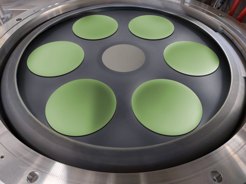
150/200 mm high throughput epitaxy for SiC Power Electronics Dual wafer size batch reactor G10-SiC - 150 mm and 200 mm – dual wafer size capable – safeguard your investment into the future - Highest wafer output / m 2 in the market - Lowest cost / wafer in the market - Excellent run-to-run process performance - Highly uniform, low defect SiC epitaxy processes for maximum chip yield Planetary Reactor® for 9 x 150 mm & 6 x 200 mm Your benefits - Single wafer performance in batch configuration - Best in class productivity - Best in class epi cost Our solutions - Fully automated wafer loading (C2C) - Individual wafer Gas Foil Rotation (GFR) - Automated Top side wafer Temperature Control (TTC) for optimized batch processing - Largest reactor capacity (9 x 150 mm & 6 x 200 mm) - High growth rate SiC processes - Hot wafer transfer and fast thermal reactor cycling - Best in class wafer throughput per m2 fab space efficacy - Low consumable cost per wafer - Highest efficiency in gas & power consumption per wafer G10-SiC: 200 mm uniformity G10-SiC: 150 mm uniformity
CATEGORY
