By EV Group
Fusion or direct wafer bonding enables permanent connection via dielectric layers on each wafer surface used for engineered substrate or layer transfer such as backside illuminated CMOS image sensors. Hybrid bonding extends fusion bonding with embedded metal pads in the bond interface, allowing for face-to-face connection of wafers. The main application for hybrid bonding is in advanced 3D device stacking.
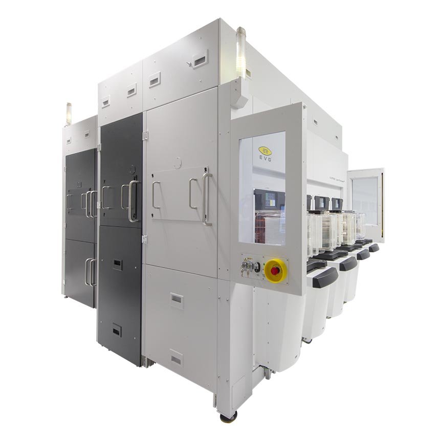
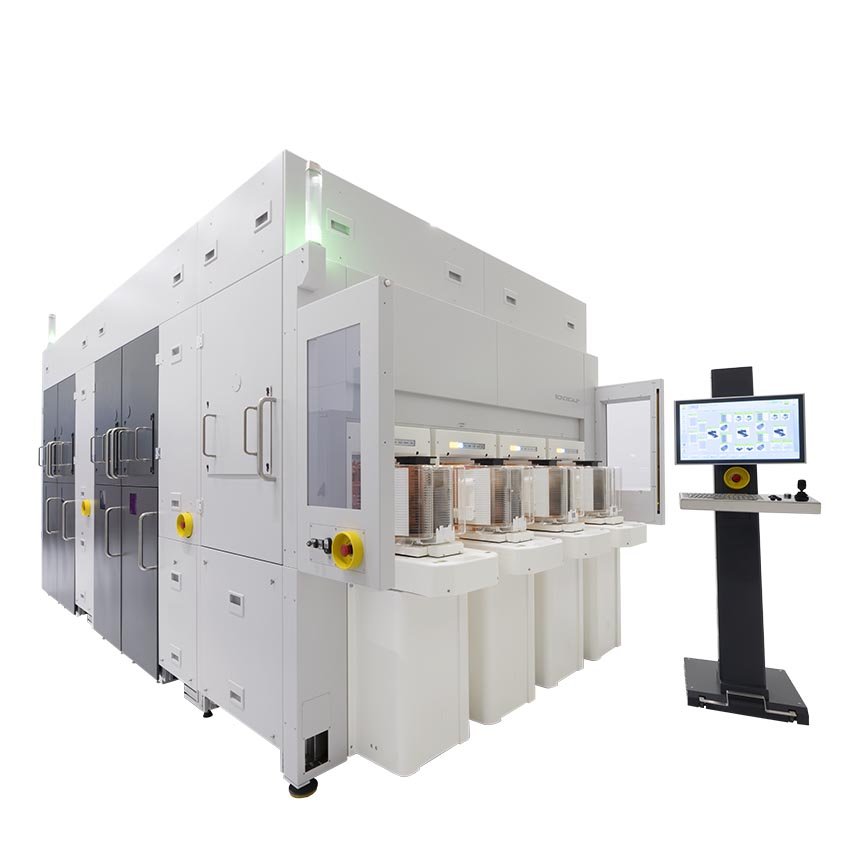
Automated Layer Release System The EVG®880 LayerRelease™ System is a fully automated system and enables precise release of layers from silicon carrier substrates using an IR laser. The EVG®880 LayerRelease™ System enables nanometer–precision release of bonded, deposited or grown layers from silicon carrier substrates using an infrared (IR) laser coupled with specially formulated inorganic release materials in a proven, high–volume–manufacturing (HVM) capable platform. The innovative process eliminates the need for glass substrates and organic adhesives overcoming the temperature limitations resulting in front–end process compatibility for ultra–thin layer transfer and downstream processes. Enabling silicon carriers with inorganic release layers avoids these temperature and glass carrier compatibility issues. In addition, the nanometer precision of IR laser-initiated separation allows for processing extremely thin device wafers without changing processes of record. Subsequent stacking of such thin device layers enables higher–bandwidth interconnects and new opportunities to design and segment dies for next–generation, high–performance devices. The EVG 880 LayerRelease System is based on the same platform as EVG’s industry–leading EVG®850 series of automated temporary bonding/debonding and silicon–on–insulator (SOI) bonding systems, with a compact design and HVM proven wafer handling system. Product Features - Fully automated, front end compatible HVM equipment. - Substrate size up to 300 mm (SEMI M1). - Substrate ID reader and SECS/GEM integration. - ISO 3 environment. - Complete process control including laser metrology at point of use. - Integrated Separation Module for separation of exposed substrates. 3D Integration | Scaling Roadmap: - Scalpel-like precision of IR laser triggered film release through silicon wafers - Enables novel, revolutionary 3D integration process flows for ultra-thin layer stacking by fusion and hybrid bonding - Integrates with any hybrid and fusion bonding process combination for advanced device manufacturing and 3D stacking - Use of existing FEOL materials, processes and infrastructure - Transfer layer uniformity is defined by epitaxy uniformity eliminating uniformity limitations from standard wafer thinning processes such as wafer grind, polish and etching - Universal material transfer in combination with fusion bonding of III-Vs, 2D materials, superlattices, etc. Heterogeneous Integration: - Enabling silicon carrier wafers as temporary carriers - Enables use of standard and established process technology, eliminating the need for adapted low temperature processes due to carrier triggered temperature limitations - Enables Processing of ultrafine pitch redistribution layer patterning on silicon substrates with leading lithography methods - No need for costly equipment updates or backside deposition to enable glass wafer processing and chucking
CATEGORY
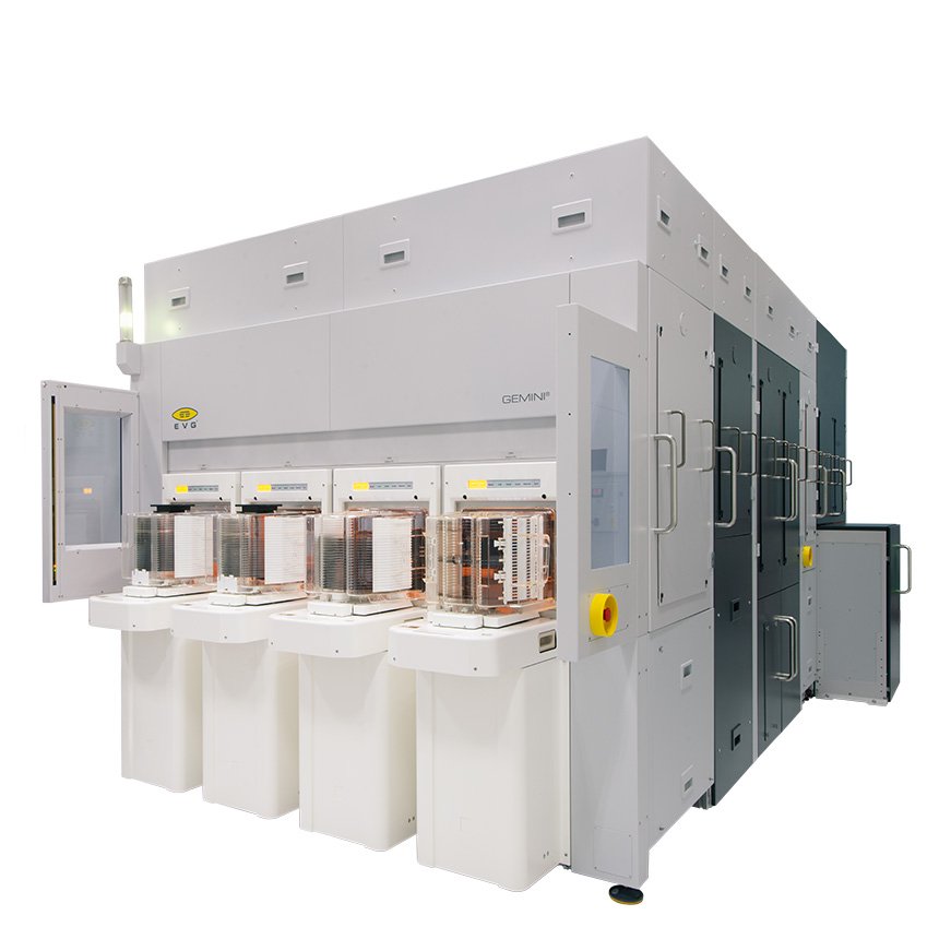
Automated Production Wafer Bonding System Integrated modular high-volume manufacturing system for aligned wafer bonding The GEMINI is a state-of-the-art, fully automated production wafer bonding system that integrates wafer-to-wafer alignment and bonding processes in a modular design. This platform is particularly suited for next-generation MEMS(Micro-Electro-Mechanical Systems) manufacturing up to 300 mm, offering exceptional performance in wafer-level vacuum or overpressure encapsulation but also in advanced system integration. Based on the global industry standard for high-volume-manufacturing (HVM) wafer bonding, the GEMINI equipment platform includes up to four bond chambers that ensure excellent bond quality and yield. The equipment provides full flexibility and supports a wide range of processes, including metal, anodic, glass-frit, fusion, and adhesive bonding. Features - Fully automated and integrated wafer bonding platform - Field-proven SmartView® bond alignment system - Bond force up to 350 kN - High bond pressure uniformity - Rapid heating and cooling - Optimized temperature uniformity - High vacuum and overpressure capability - Accurate chamber pressure control - Modular concept for full process flexibility - Smart process control and data analysis - Simplified, user-friendly interface Technical Data 200 mm GEMINI® - Wafer sizes from 100 mm to 200 mm - Bond force up to 100 kN - Up to 4 bond modules - Overpressure capability up to 3000 mbar - Different system layouts with up to 4 pre-process modules - EVG load ports or SMIF load ports 300 mm GEMINI® - Wafer sizes from 200 mm to 300 mm - Bond force up to 350 kN - Up to 4 bond modules - Overpressure capability up to 2000 mbar - Different system layouts with 2 to 6 pre-process modules - FOUP load ports (optional adapter for 200 mm substrates) - EFEM
CATEGORY
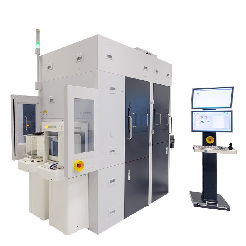
Multifunctional UV Nanoimprint Lithography System. Multifunctional UV Nanoimprint Lithography system up to 300mm featuring SmartNIL®technology, lens molding and lens stacking in one tool.
CATEGORY
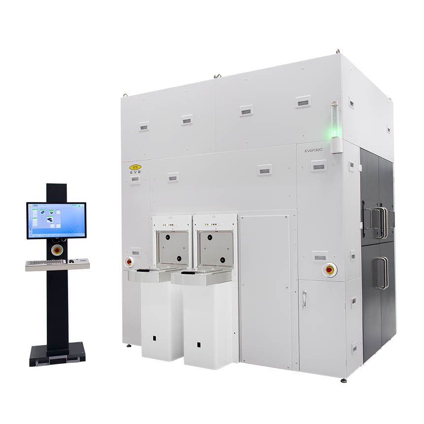
Automated Single Wafer Cleaning System Automated single wafer cleaning system for efficient removal of particles The EVG320 automated single wafer cleaning system handles wafers and substrates automatically between the process stations. The robot handling system ensures pre-alignment and loading of the wafers automatically in a cassette-to-cassette or FOUP-to-FOUP operation. Features - Available for aqueous based cleaning applications such as silicon direct bonding - Available for solvent based cleaning applications such as post-debond cleans - Up to four cleaning stations - Fully automated cassette-to-cassette or FOUP-to-FOUP handling - Edge handling for double-sided cleaning processes available (option) - High-efficiency cleaning using 1 MHz megasonic nozzles or area transducers (option) - Advanced remote diagnostics - Prevents cross-contamination from back to front side - Fully software-controlled cleaning process Technical Data Wafer diameter (substrate size) 200, 100 - 300 mm Cleaning system Open chamber, spinner and cleaning arm Chamber: made of PP or PFA (option) Cleaning media: DI-water (standard), other cleaning media (option) Spinner chuck: vacuum chuck (standard) and edge handling chuck (option) made of metal ion free and clean materials Rotation: up to 3000 rpm (in 5 sec) Megasonic nozzle Frequency: 1 MHz (3 MHz option) Output power: 30 - 60 W DI-water flow rate: up to 1.5 liter/min Effective cleaning area: Ø 4.0 mm Material: PTFE Megasonic area transducer Optional Frequency: 1 MHz (3 MHz option) Output power: max. 2.5 W/cm² active areas (max. output 200 W) DI-water flow rate: up to 1.5 liter/min Effective cleaning area: triangle shape that guarantees radio uniformity on whole wafers per each rotation Material: SS and sapphire Brush Material: PVA Programmable parameters: brush and wafer speed (rpm) Adjustable parameters (brush compression, media dispense) Automated wafer handling system The field proven class 1 compatible wafer handling robot on EVG ® 320 enables 24 hour automated cassette-to-cassette or FOUP-to-FOUP operation for the highest throughput. Surfaces in contact with wafers do not cause any metal ion contamination. Optional features ISO 3 mini-environment (according to ISO 14644)
CATEGORY
