By XTPL
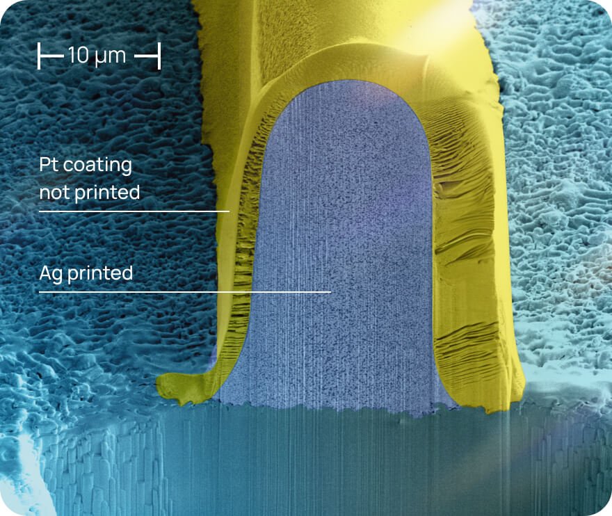
High-Performance Materials benefits: Superior stability; Up to 50% silver bulk conductivity; High content of conductive component. Over 40% of bulk silver conductivity. Non-clogging behavior for long continuous printing times. Compatible with various substrates including flexible polymers. Compatible with multiple inkjet printhead types. Typical properties — Silver content [wt. %]: 34 ± 2; Average nanoparticles size [nm] (TEM): 35 - 50; Shape of nanoparticles: Spherical; Electrical resistivity [μΩ · cm]*: <3.95 (ca. 41% Ag bulk conductivity); Viscosity (25°C) [cP]: 26 - 30 (SR = 40 s -1); Solvent(s): Glycol ether; Compatible printing method: • Inkjet.
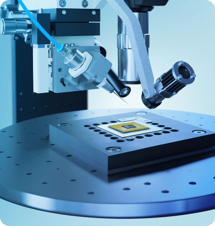
Explore our Open Prototyping Platform, delivering reliable, repeatable, and durable results for high performance materials. Easy to operate and maintain. Ideal tool for R&D in various microelectronics applications. Proven one-stop-shop in R&D and commercial settings Delta Printing System - Stand-alone, open platform - For prototyping and small-volume/nest production - Freedom of control over printhead - Flexibility of user Interface: manual mode, CAD import, advanced scripting - Fast & easy exchange of cartridges & nozzles XTPL® Software - Intuitive navigation: icons, toolbars, and other visual elements provide clues and make it easier to understand app features - Increased productivity & minimize errors: with visual cues and easier navigation, users are less likely to make mistakes - Faster access to features: well-designed software allows to quickly find and use the features Suitable for various applications, such as: - 3d interconnections - Advanced IC packaging - RDL prototyping - TSV filling DPS provides: - High aspect ratios in a single pass benefit memory chips and MEMS - No overflow or spills - Reduced production costs - Convenient cartridge and nozzle exchange - High density interconnections down to 1 µm / 1 µm L/S TFT arrays: - Prototyping TFT and electrical circuit - Open defects repair - No risk to damage discreate elements by eliminating electrical field - Conductive structures down to 1µm Quantum Dots Printing: - DPS supports printing with Quantum Dots-based inks (QD inks) - Its versatility is crucial for OLED and microLED - With printed QD inks having a dimension of 3.5 µm width and below 300nm height, offers time and material savings and precision Delta addresses specific challenges in the prototyping and fabrication of modern PCBs: - Ultra-high resolution printing and feature sizes of 1‑10 μm tackles the design complexity and enables the creation of specific PCB structures - Versatility allows for the integration of diverse materials, both conductive and non-conductive, while maintaining high aspect ratios in a single pass We ensure: - Printing on 3D topographies feature uniformity - The reliability and performance of the PCBs - A comprehensive solution for modern PCB manufacturing Our innovative biosensor solution: - High performance - Size reduction - Cost-effective fabrication methods - Groundbreaking for rapid biosensor prototyping - Enables biosensing patterns on flexible substrates, crucial for wearable sensors Delta system ensures: - Uniform, clean features without spills crucial for intricate biosensor designs - Maintaining reliability and accuracy Our technology Printing on the edge Printing on the edge - Edge interconnections printing - High resolution traces, below 10 µm - Possibility to print over the edge of glass, silicon and flexible foils RDL Redistribution layer prototyping - All printed RDL structure - Down to 1 μm / 1 μm L/S density - Variable materials possible to use in one system, for example metallic nanoparticle paste and high viscous polyimide Chip interconnection Chip interconnection - Reliable connection for flexible hybrid electronics and advanced IC packages - High density interconnections on stacked chips - Resolution <10 μm/10 μm L/S - No satellite droplets and line width homogeneity to prevent electrical shorts Achieve unparalleled accuracy Prototype microelectronic devices with exceptional precision using our XTPL® Delta Printing System and high-viscosity conductive inks.
CATEGORY
Printhead The innovative head is the heart of XTPL's microprinting system. It works on the basis of a unique algorithm and enables ultra-precise ink application. Customized, integrated printing engine UPD System - Integration with running production lines - Suitable for continuous/flow line production - Small to high volume production - Compatible with DPS accessories and materials - Easy change over of cartridge and nozzles - Single or multi-nozzle compatible Features of printing head - Allowing defects in conductive paths to be repaired at low cost, with precision and speed - Conductive traces can be obtained with a single pass of printing head - We provide unique printing heads – designed and dedicated for specific application fields Highly precise structures Precision and accuracy Ultra Precise Dispensing System guarantees unparalleled precision and accuracy in dispensing nanomaterials, leading to the creation of highly precise conductive and nonconductive structures Wide range of materials Material versatility and compatibility The system accommodates a wide range of nanomaterials, ensuring compatibility with diverse conductive and nonconductive substances for the production of specialized structures and coatings Tailor-made solutions Customization and flexibility Tailored dispensing parameters and configurations offer adaptability, enabling manufacturers to meet specific production requirements and diverse applications Accelerate the process High throughput Integrated seamlessly into production lines, the dispensing system enhances throughput, enabling faster manufacturing without sacrificing precision Manufacturing on any scale Scalability Serving as a one-stop solution, the dispensing system is scalable for diverse production scales, ranging from small batches to large-scale manufacturing Even higher efficiency Reduced production downtime The reliable and robust Ultra Precise Dispensing System minimizes downtime, improving overall production efficiency and output Enhancing system functionality Expert Engineering Support Top-notch engineering services provide manufacturers with expert guidance, support, and troubleshooting during integration, optimizing overall system performance Innovative print technology XTPL print head ensures the width of printed structures reaches up to 1 µm. It also allows printing on most surfaces, including flexible or curved ones.
CATEGORY
XTPL® Software - Intuitive navigation: icons, toolbars, and other visual elements provide clues and make it easier to understand app features - Increased productivity & minimize errors: with visual cues and easier navigation, users are less likely to make mistakes - Faster access to features: well-designed software allows to quickly find and use the features
CATEGORY
Conductive gold nanopaste highlights The Intended Use case for Au Nanopaste 90 Designed for application in printed electronics, especially for fine feature printing and deposition of electrodes for sensor applications With our new product, we maintain our commitment to combine fine feature printing and highly concentrated formulations, a hallmark of our expertise. Features a nanoparticle-based composition, with nanoparticles predominantly in spherical shape Can be printed on different substrates such as glass, PCB material and foils (e.g. PET, Kapton) Designed with unmatched anti-clogging properties, ideal for the deposition of fine features This product is only intended to be used as an accessory for Delta Printing System device. This product is intended to store and dispense Au90 paste used in additive manufacturing. Use of different inks and pastes must be consulted with XTPL. The cartridge must be used only with XTPL nozzles. This product should not be used for injection of any materials. This product is intended for professional use. Modifications during technological progress are reserved. The device is not intended for pharmaceutical, healthcare, medical device nor household uses. The ink (paste) is not intended to be in contact with operator. This product is designed for use as a key component in the manufacturing of conductive patterns and structures. It is also suitable for creating electronic circuits and devices on cost-effective, disposable substrates. The formulation of this product includes a paste with a specific viscosity greater than 100 000 cP at a shear rate of 0.2 1/s at 25 °C, composed of highly concentrated (87 ± 2 wt.%) gold nanoparticles (35-55 nm in size) within a specialized container. The paste’s conductivity is rated from 25% of bulk gold after sintering 20 min at min. 350°C in the oven. This product is strictly not for use in pharmaceutical, healthcare, medical device, or household applications. Usage must be in strict accordance with the Material Safety Data Sheet (MSDS). Exhibits enhanced metal loading resulting in a substantial amount of conductive component dispensed in a single pass Compatible with XTPL Utra-Precise Dispensing (Former Ultra-Precise Deposition) For cartridge For paste The images depict reference views, which vary depending on the product application method, and do not constitute a guarantee of the printout parameters or outcomes. Avoid skin and eye contact, XTPL Au Nanopaste 90 can cause eye and skin irritation. If ingested, consult a physician immediately. Before using the product read the Material Safety Data Sheet (MSDS) and product label: Use appropriate safety equipment (e.g. latex gloves, safety glasses). Wash hands thoroughly after handling. Safety and handling Shelf-life Keep away from sunlight or other direct light sources. Store in between 4 – 6 °C, do not freeze. Allow closed container to stabilize at room temperature prior to opening and use. Minimize exposition of open container to external atmosphere to a maximum (prevention of solvent evaporation and spilling hazard). Technical Data Sheet Reference applications Material: Gold nanoparticles 90% Shape: Spherical Solid content [wt. %] (2h, 185 °C): 90 ± 3 Gold content [wt. %]: 87 ± 2 Average nanoparticles size [nm] (DLS): 80 – 130 Average nanoparticles size [nm] (TEM): 35 – 55 Electrical resistivity [μΩ · cm]: 8.13 (27% Au bulk conductivity) Viscosity (25°C) [cP]: 100 000 (SR = 0,2 s -1 )Glycol(s) Solvent(s): Glycol(s) Storage conditions: 4 – 6 °C; stored away from sunlight or other direct light sources Shelf life (under given storage recommendations): 2 months MSDS in English: Attached to the product and available upon request Au Nanopaste 90 parameters Value Sintering conditions: 350 °C; 20 minutes; Air Product specification SEM images of conductive lines printed with Au Nanopaste 90 Cross-section Pt Au Glass Top view The featured product is under active development. Provided product information is based on present knowledge and experience. Information related to feature(s) of the product do not guarantee similar achievable results.We reserve the right to make any changes according to further developments or investigations. Product not intended for clinical use. Dispensing Used abbreviations DLS Dynamic Light Scattering TEM Transmission Electron Microscopy SEM Scanning Electron Microscopy
CATEGORY
