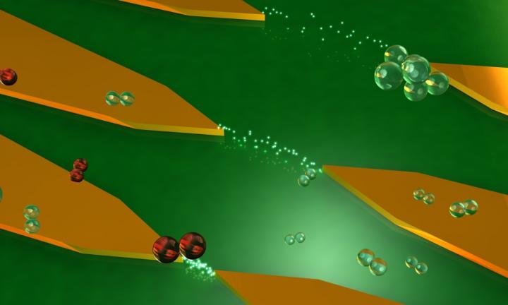
Researchers at RMIT University have engineered a new type of transistor, the building block for all electronics. Instead of sending electrical currents through silicon, these transistors send electrons through narrow air gaps, where they can travel unimpeded as if in space.
The device unveiled in material sciences journal Nano Letters, eliminates the use of any semiconductor at all, making it faster and less prone to heating up.
Lead author and PhD candidate in RMIT's Functional Materials and Microsystems Research Group, Ms Shruti Nirantar, said this promising proof-of-concept design for nanochips as a combination of metal and air gaps could revolutionise electronics.
"Every computer and phone has millions to billions of electronic transistors made from silicon, but this technology is reaching its physical limits where the silicon atoms get in the way of the current flow, limiting speed and causing heat," Nirantar said.
"Our air channel transistor technology has the current flowing through air, so there are no collisions to slow it down and no resistance in the material to produce heat."
The power of computer chips - or number of transistors squeezed onto a silicon chip - has increased on a predictable path for decades, roughly doubling every two years. But this rate of progress, known as Moore's Law, has slowed in recent years as engineers struggle to make transistor parts, which are already smaller than the tiniest viruses, smaller still.
Nirantar says their research is a promising way forward for nano electronics in response to the limitation of silicon-based electronics.
"This technology simply takes a different pathway to the miniaturisation of a transistor in an effort to uphold Moore's Law for several more decades," Shruti said.
Research team leader Associate Professor Sharath Sriram said the design solved a major flaw in traditional solid channel transistors - they are packed with atoms - which meant electrons passing through them collided, slowed down and wasted energy as heat.
"Imagine walking on a densely crowded street in an effort to get from point A to B. The crowd slows your progress and drains your energy," Sriram said.
"Travelling in a vacuum on the other hand is like an empty highway where you can drive faster with higher energy efficiency."
But while this concept is obvious, vacuum packaging solutions around transistors to make them faster would also make them much bigger, so are not viable.
"We address this by creating a nanoscale gap between two metal points. The gap is only a few tens of nanometers, or 50,000 times smaller than the width of a human hair, but it's enough to fool electrons into thinking that they are travelling through a vacuum and re-create a virtual outer-space for electrons within the nanoscale air gap," he said.
The nanoscale device is designed to be compatible with modern industry fabrication and development processes. It also has applications in space - both as electronics resistant to radiation and to use electron emission for steering and positioning 'nano-satellites'.
"This is a step towards an exciting technology which aims to create something out of nothing to significantly increase speed of electronics and maintain pace of rapid technological progress," Sriram said.
This work was undertaken at RMIT University's cutting-edge Micro Nano Research Facility and with support of the Victorian node of the Australian National Fabrication Facility.
The article is now available online DOI: 10.1021/acs.nanolett.8b02849
RMIT University
#Nanoelectronics
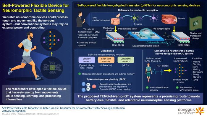
The proposed TENG-driven g-IGT is a flexible, self-powered neuromorphic device capable of reproducing multiple memory states and spike-rate-dependent learning Neuromorphic devices, which are designed to emulate aspects of biological neural networks, are promising candidates for developing low-power and intelligent sensing technologies, including wearable applications. Among the device architectures explored for neuromorphic computing, graphene-channel ion-gel-gated transistors (g-IGTs) are...
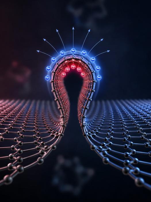
Rice University researchers have shown that sub-nanometer wrinkles in graphene generate flexoelectric charge separation, reshaping local electrical behavior through curvature alone. Extreme bending produces polarization far stronger than in larger systems and may enable geometry-controlled electronics without chemical doping. Published in Advanced Materials.
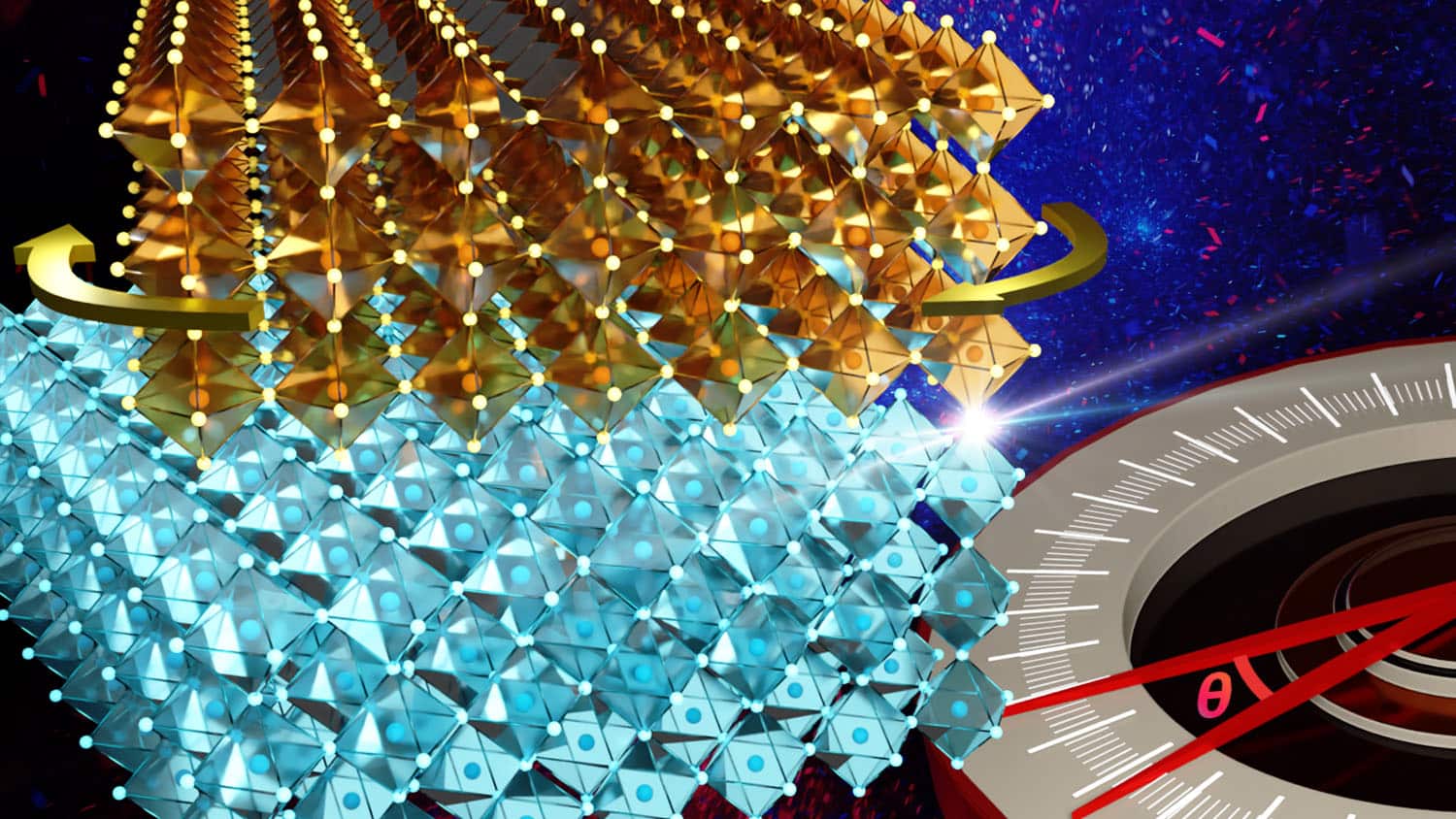
Researchers at NC State have extended twistronics beyond van der Waals materials into strongly bonded crystalline oxides. By stacking sodium niobate membranes with twist angles controlled down to 0.1 degrees, and confirming results via synchrotron X-ray diffraction, the team found interlayer bonds distort the atomic lattice, shifting phase structure and domain configuration. The technique works at near-millimeter scale, far larger than typical twistronic devices, marking a real step toward pract
