
A team of researchers from Russia, Great Britain, Japan, and Italy has created a graphene-based terahertz detector. The study was published in Nature Communications.
Any system for wireless data transfer relies on electromagnetic wave sources and detectors, but they are not available for every kind of waves. The existing sources of terahertz radiation, which occupies a middle ground between microwaves and infrared light, consume too much power or require intense cooling. Yet T-waves could potentially enable faster Wi-Fi, new methods of medical diagnostics, and studies of space objects using radio telescopes.
The reason for the inefficiency of the existing terahertz detectors is the mismatch between the size of the detecting element, the transistor -- about one-millionth of a meter -- and the typical wavelength of terahertz radiation, which is some 100 times greater. This results in the wave slipping past the detector without any interaction.
In 1996, it was proposed that to address this issue, the energy of an incident wave could be compressed into a volume comparable to the size of the detector. For this purpose, the detector material should support "compact waves" of a special kind, called plasmons. They represent the collective motion of conduction electrons and the associated electromagnetic field, not unlike the surface sea waves moving together with the wind as a storm sets in. In theory, the efficiency of such a detector is further increased under wave resonance.
Implementing such a detector proved harder than anticipated. In most semiconductor materials, plasmons undergo rapid damping -- that is, they die down -- due to electron collisions with impurities. Graphene was seen as a promising way out, but until recently, it was not clean enough, too.
The authors of the research presented a solution for the long-standing problem of resonant T-wave detection. They created a photodetector made of bilayer graphene encapsulated between crystals of boron nitride and coupled to a terahertz antenna. In this sandwich structure, impurities are expelled to the exterior of the graphene flake, enabling plasmons to propagate freely. The graphene sheet confined by metal leads forms a plasmon resonator, and the bilayer structure of graphene enables wave velocity tuning in a wide range.
In fact, the team has developed a compact terahertz spectrometer, several microns in size, with the resonant frequency controlled via voltage tuning. The physicists have also shown the potential of their detector for fundamental research: By measuring the current in the detector at various frequencies and electron densities, plasmon properties can be revealed.
"Our device doubles up as a sensitive detector and a spectrometer operating in the terahertz range, and it's also a tool for studying plasmons in two-dimensional materials. All of these things existed before, but they took up a whole optical table. We packed the same functionality into a dozen micrometers," said the paper co-author Dmitry Svintsov.
Resonant terahertz detection using graphene plasmons
Denis A. Bandurin, Dmitry Svintsov, Igor Gayduchenko, Shuigang G. Xu, Alessandro Principi, Maxim Moskotin, Ivan Tretyakov, Denis Yagodkin, Sergey Zhukov, Takashi Taniguchi, Kenji Watanabe, Irina V. Grigorieva, Marco Polini, Gregory N. Goltsman, Andre K. Geim & Georgy Fedorov
Nature Communications vol. 9, no.: 5392 (2018)
DOI: 10.1038_s41467-018-07848-w
Contact information:
Dmitry Svintsov
MIPT, Laboratory of 2D Materials for Optoelectronics
svintcov.da@mipt.ru
Moscow Institute of Physics (MIPT)
#Graphene #Transistors #Plasmonics
SPECS reports on work at the LMA microscopy lab, where Dr. David Serrate's team used the JT-STM to study graphene nanoribbons on MgO/Ag(001) and the Aarhus 150 to monitor nanostructure growth.
Nanologica's board has resolved on a rights issue of units of appx. SEK 110.5 million, with an oversubscription option of up to SEK 10 million. Commitments and a guarantee intention cover appx. SEK 85.7 million.
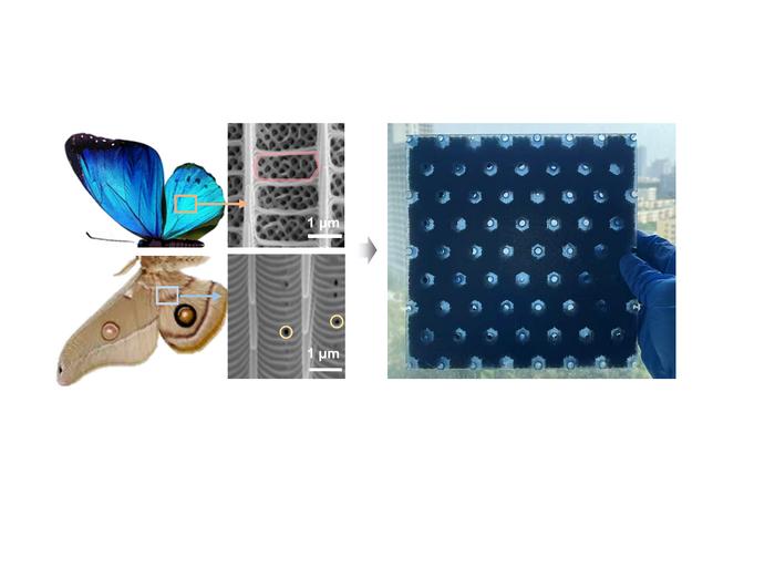
Researchers at Harbin Institute of Technology have printed a 24 mm metamaterial that absorbs impact, shields microwaves and damps low-frequency noise at once. Inspired by butterfly wing scales, it nests a gyroid lattice inside a hexagonal honeycomb, absorbing 21.9 times more impact energy than an equal-weight honeycomb and capturing over 90% of 2-40 GHz radiation and 600-900 Hz sound.
This week in nanotech
$105.3M raised
6 funding rounds · 35 deals tracked
New products
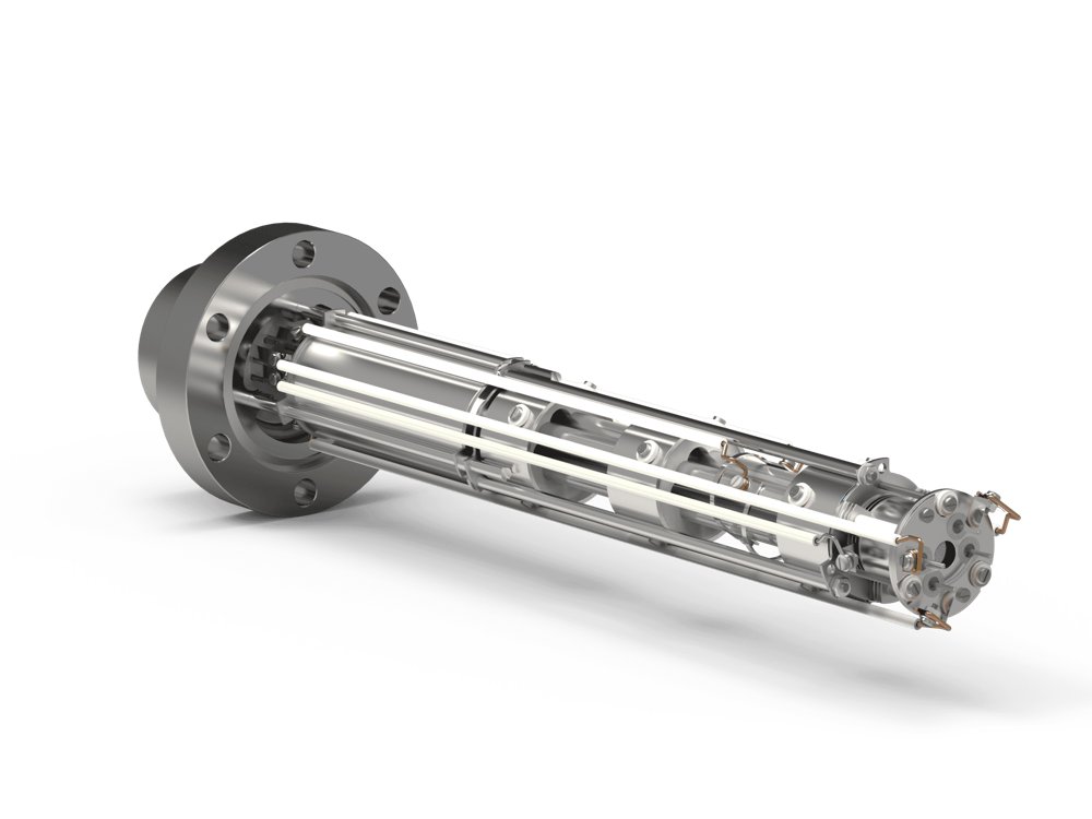 DLS-1 Mass Spectrometer for Fusion Gas AnalysisHiden Analytical Featured
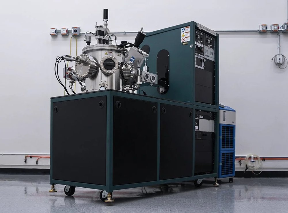 Orion Sputtering Deposition SystemsAJA International Featured
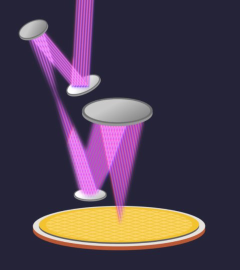 Aether®Lam Research
Market insights
Last 30 days: Quantum Technologies drew the most money: $3.17B.
Money raised per month
Behind the deal
Who invested in Vertical Semiconductor’s $73M Grant?
See the investors with Insights Pro →