Los Gatos, 22 October 2026. Atomera has entered into a Joint Development Agreement (JDA) with IQE plc to bring high-performance, cost-effective RF GaN to market. Atomera is a semiconductor transistor materials and technology licensing company based in Los Gatos, California. IQE supplies compound semiconductor wafer products and advanced material solutions.
The collaboration combines Atomera's recently announced application of Mears Silicon Technology (MST) to silicon substrates for RF GaN with IQE's compound semiconductor epitaxy expertise. Under the agreement, the companies will work to demonstrate GaN epitaxy on Atomera's MST-enabled silicon wafers. The initial focus is RF GaN-on-silicon applications, aiming to demonstrate best-in-class linearity and loss for high-volume RF markets.
The companies anticipate a multi-cycle development process, with engineering teams from both working together to optimize the multi-layer structure and identify the highest-performing RF material. The project will center on production and testing of MST-enabled GaN-on-silicon wafers. The goal is to make samples available for foundry, IDM and fabless customer engagement. IQE will manufacture the wafers for foundry and IDM customers.
The JDA leaves room for the companies to expand their work, both to further refine RF GaN and to pursue other GaN use cases, including power electronics.
"IQE has built its business on delivering compound semiconductor epitaxy that meets the industry's highest performance bar, and this collaboration with Atomera is a natural extension of that work," said Dr. Rodney Pelzel, chief strategy and technology officer at IQE.
"GaN has become critical to RF and power applications, but bringing high-performance GaN to volume production at a cost that works for mainstream markets remains a real challenge," said Scott Bibaud, president and CEO of Atomera. MST is a quantum-engineered epitaxial silicon material that enhances transistors and, when applied to GaN epitaxy, enables improved RF GaN performance on silicon substrates.
Source: Atomera news
Polar Semiconductor and IC-Link by imec are collaborating on 8-inch production of enhancement-mode GaN devices, enabled by a license transfer agreement with imec for its GaN-on-silicon process, device and epitaxy.
SPECS reports on work at the LMA microscopy lab, where Dr. David Serrate's team used the JT-STM to study graphene nanoribbons on MgO/Ag(001) and the Aarhus 150 to monitor nanostructure growth.
JEDEC has set the first silicon photonics AI network reliability standard, according to the feed headline.
This week in nanotech
$108.5M raised
8 funding rounds · 46 deals tracked
New products
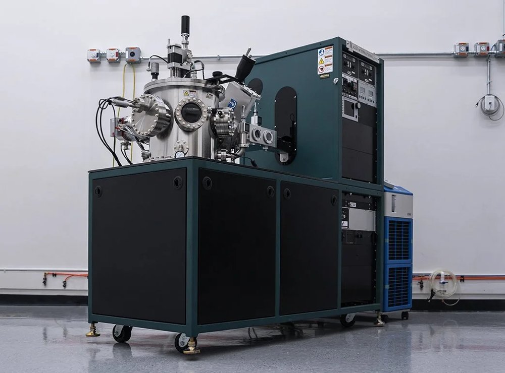 Orion Sputtering Deposition SystemsAJA International Featured
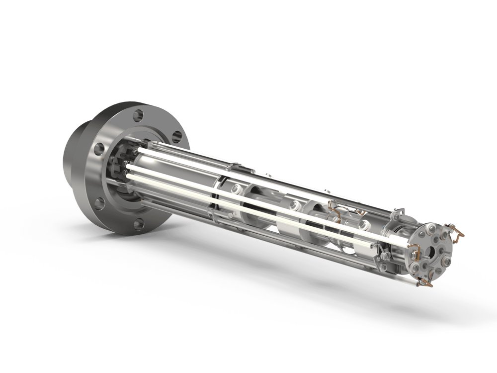 DLS-1 Mass Spectrometer for Fusion Gas AnalysisHiden Analytical Featured
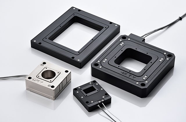 PKVH / PKVL ZAxis With an opening modelTHK PRECISION CO.,LTD.
Market insights
Last 30 days: Quantum Technologies drew the most money: $3.17B.
Money raised per month