
Researchers have fabricated a quasi-one-dimensional van der Waals zirconium telluride thin film, which is a form of a substance that has long promised advances in quantum computing, nano-electronics and other advanced technologies. Until now, it has stumped scientists who have tried to manufacture it in large-scale quantities.
A paper describing a new fabrication technique was published in the Journal of Materials Science & Technology on June 8, 2024.
Quasi-one-dimensional (quasi-1D) van der Waals materials have become a hot topic in materials science research in recent years for their unique structure's quantum effects that produce unusual electrical, optical and mechanical properties. They are referred to as "quasi" 1D substances because while the molecules in true 1D materials are chains linked by covalent chemical bonds, in quasi-1D materials, extremely weak intermolecular forces--known as Van der Waals forces--between these 1D chains also arrange them into 2D sheets. This combines the advantages of 1D substances' ability to amplify quantum effects with the advantages of stackable 2D sheet materials.
As a result of this one-two punch, quasi-1D materials are widely viewed as critical to the development of the next generation of nano-electronics, quantum computing, spintronics and other bleeding-edge technologies.
Zirconium pentatelluride (ZrTe₅) has recently attracted attention as a material due to its properties as a Dirac and Weyl semimetal--where the electrons behave as though they have zero mass, and so enjoy even more exotic optical and magnetic properties.
"Unfortunately, until now, due to the difficulty of large-scale manufacturing of ZrTe₅ films, this wonder substance has remained something of a lab-bench novelty," explains Yi Shuang of the WPI Advanced Institute for Materials Research (WPI-AIMR) at Tohoku University.
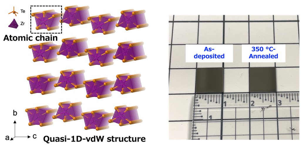
Researchers turned to an alternative method for thin film fabrication: physical vapor deposition (PVD). Specifically, they employed PVD "sputtering." In this context, sputtering doesn't mean the explosive sounds of a dying engine. Rather, sputtering refers to the bombardment of a target substance by atoms or ions resulting in an ejection of material from that target and onto another substance or "substrate." PVD sputtering is well-established as a manufacturing process in the semiconductor industry.
The researchers used an RF magnetron--a device that uses radio frequency energy to produce the sputtering effect--on zirconium and tellurium targets at the same time. Large-scale growth of quasi-1D ZrTe₅ was achieved.
Immediately upon deposition of the ZrTe₅ on the substrate, the films were initially in an amorphous state. However, upon heat treatment in an argon atmosphere, crystallization then occurred, leading to a dramatic change in the material's properties. This transition is crucial for obtaining the specific characteristics necessary for the desired quasi-1D ZrTe₅ applications.
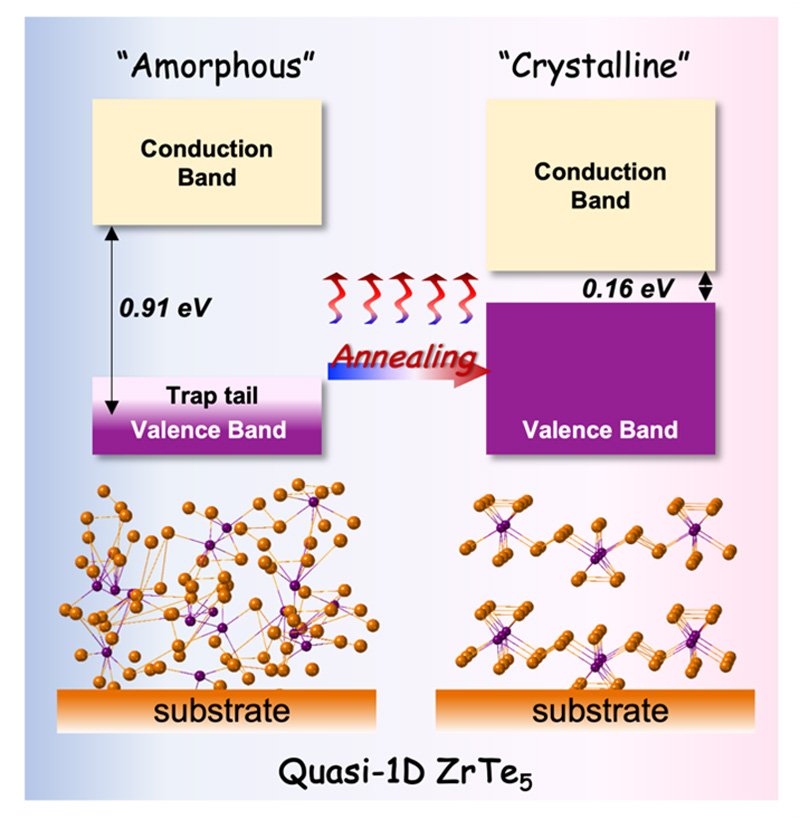
A detailed analysis of this transformation from amorphous to crystalline structure revealed why this happens. In so doing, the research team advanced the fundamental understanding of amorphous-to-crystalline phase transition in quasi-1D materials in general, not just of ZrTe₅. The team now aims to refine this analysis of the crystallization process using other advanced techniques, as well as test the performance of the material's performance in real-world applications.
Reference
Amorphous-to-crystalline transition-induced two-step thin film growth of quasi-one-dimensional penta-telluride ZrTe₅
Yi Shuang, Yuta Saito, Shogo Hatayama, Paul Fons, Ando Daisuke, Yuji Sutou
https://www.sciencedirect.com/science/article/pii/S1005030224006182

Waste polyamide-derived CQDs show continuous photoluminescence tuning from 308 to 552 nm through sequential defect-state engineering, with optical transition energies decreasing from 4.32 to 2.50 eV. @Christian Ebere Enyoh from Saitama University Carbon quantum dots (CQDs) are fluorescent carbon nanomaterials with potential applications in sensing, optoelectronics, displays, anti-counterfeiting, and environmental technologies. Their optical properties can be adjusted by modifying the carbon...

The researchers used circularly polarized light at normal incidence and found that helicity-dependent photocurrents appeared perpendicular to the crystal’s polarization but vanished when measured parallel to it, supporting a bulk origin of CPGE. @Institute of Science Tokyo The circular photogalvanic effect (CPGE), a phenomenon that generates helicity-dependent photocurrents in noncentrosymmetric materials, can originate purely from a crystal's internal structure without contribution from the...

Summary of gold nanoparticle growth programming in liposome based on localization of biomineralization peptide The position of biomineralization peptides within liposomes can influence how gold nanoparticles grow, reports a research team from Institute of Science Tokyo. Peptides localized at the membrane interface promote branched structures, while those confined to the liposome interior favor spherical nanoparticles. The findings offer a new strategy for controlling nanoscale reaction...
