UC San Diego (UCSD)
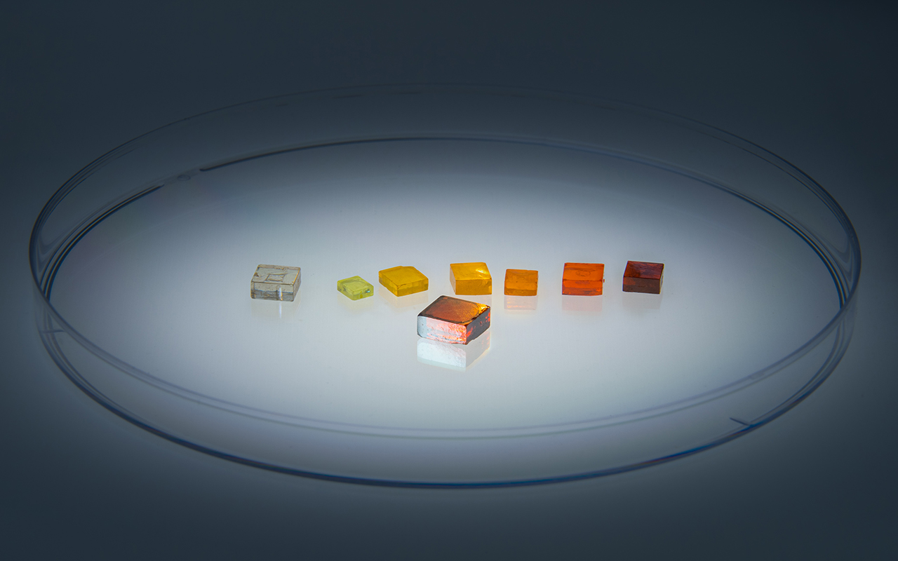
A new method could enable researchers to fabricate more efficient and longer lasting perovskite solar cells, LEDs and photodetectors. By growing thin perovskite films on substrates with different compositions, engineers at the University of California San Diego have invented a way of fabricating perovskite single crystals with precisely deformed, or strained, structures.
Engineering a small amount of strain in perovskites is of great interest because it provides a way to make significant changes in the material's properties, such as how it conducts electricity, absorbs and transmits light, or how stable it is.
"You can use strain engineering as a knob to tune existing functions or even install new functions in a material," said Sheng Xu, a professor of nanoengineering at the UC San Diego Jacobs School of Engineering and the senior author of the study.
There are techniques that use heat to introduce strain in perovskite crystals, but that strain is typically short lived or uncontrollable in terms of its magnitude, which makes these strain-engineered perovskites impractical to use. Existing strain engineering techniques are also incompatible with device fabrication processes.
Xu and his team tackled these problems by carefully growing deformed perovskite single crystals. Their technique permanently embeds strain into the material's structure and allows them to tailor the amount of strain--the more deformed the crystal lattice, the higher the strain.
The type of perovskite investigated in this study is alpha-formamidinium lead iodide, which has been used to create the highest efficiency perovskite solar cells to date. The researchers grew crystals of the material on a series of perovskite substrates with varying compositions and lattice sizes--a process called heteroepitaxial growth. As the material crystallized, it adopted the lattice size of its substrate, which essentially forced the alpha-formamidinium lead iodide crystals to grow differently than they normally do.
"Thus, the lattices in the material are deformed and strained to different degrees, depending on the lattice mismatch between material and substrate," explained Yimu Chen, a nanoengineering Ph.D. student in Xu's lab and co-first author of the study.
"Because we are introducing strain at the atomic level, we can precisely design the strain and control it," said Yusheng Lei, who is also a nanoengineering Ph.D. student in Xu's lab and the other co-first author of the study.
The researchers grew perovskite crystals with five different levels of strain ranging from 0 to -2.4%. They found that -1.2% strain produced samples with the best charge-carrier mobility.
The team also reported another interesting discovery: growing alpha-formamidinium lead iodide crystals with strain stabilized its photoactive alpha phase. "In its strain-free form, alpha-formamidinium lead iodide undergoes a phase transition from a photoactive phase to a non-photoactive phase, which is bad for photovoltaic applications," Chen said. "With our growth method, we can lock the material's crystal structure with that of the substrate to prevent this phase transition and enhance its phase stability."
In future studies, the researchers will explore what new properties and functionalities they can strain engineer into perovskites using their method. They will also work on scaling up their process to grow large, single-crystalline thin films for industrial applications.
Strain engineering and epitaxial stabilization of halide perovskites
Yimu Chen, Yusheng Lei, Yuheng Li, Yugang Yu, Jinze Cai, Ming-Hui Chiu, Rahul Rao, Yue Gu, Chunfeng Wang, Woojin Choi, Hongjie Hu, Chonghe Wang, Yang Li, Jiawei Song, Jingxin Zhang, Baiyan Qi, Muyang Lin, Zhuorui Zhang, Ahmad E. Islam, Benji Maruyama, Shadi Dayeh, Lain-Jong Li, Kesong Yang, Yu-Hwa Lo & Sheng Xu
Nature volume 577, pages 209–215 (2020)
DOI: 10.1038/s41586-019-1868-x
Contact information:
Sheng Xu
Professor of nanoengineering at the UC San Diego Jacobs School of Engineering
shengxu@ucsd.edu
Phone: 858-246-0811
Xu Group @ UCSD
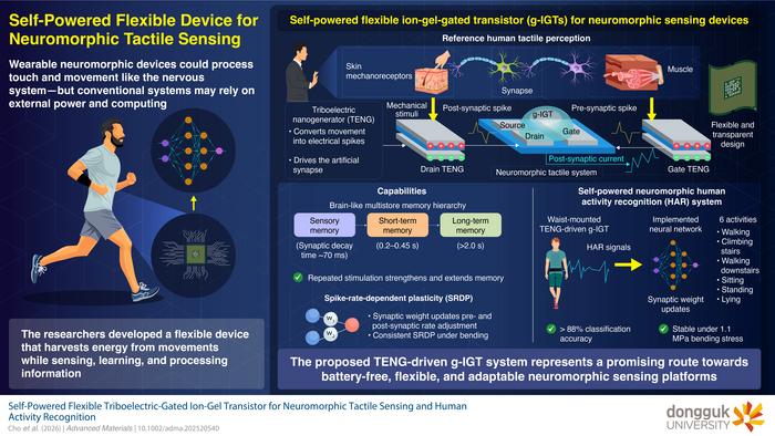
The proposed TENG-driven g-IGT is a flexible, self-powered neuromorphic device capable of reproducing multiple memory states and spike-rate-dependent learning Neuromorphic devices, which are designed to emulate aspects of biological neural networks, are promising candidates for developing low-power and intelligent sensing technologies, including wearable applications. Among the device architectures explored for neuromorphic computing, graphene-channel ion-gel-gated transistors (g-IGTs) are...
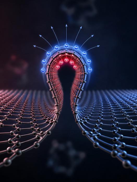
Rice University researchers have shown that sub-nanometer wrinkles in graphene generate flexoelectric charge separation, reshaping local electrical behavior through curvature alone. Extreme bending produces polarization far stronger than in larger systems and may enable geometry-controlled electronics without chemical doping. Published in Advanced Materials.
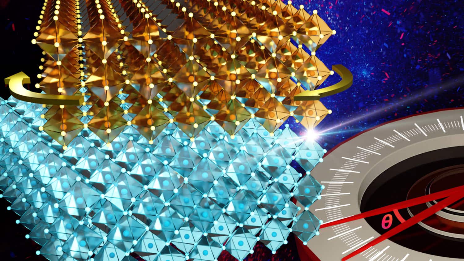
Researchers at NC State have extended twistronics beyond van der Waals materials into strongly bonded crystalline oxides. By stacking sodium niobate membranes with twist angles controlled down to 0.1 degrees, and confirming results via synchrotron X-ray diffraction, the team found interlayer bonds distort the atomic lattice, shifting phase structure and domain configuration. The technique works at near-millimeter scale, far larger than typical twistronic devices, marking a real step toward pract
