28 October 2026. NanoImages has published a decision guide for choosing among the five analytical add-ons available for its SNE-Alpha benchtop scanning electron microscope. The SNE-Alpha carries factory ports for electron dispersive spectroscopy (EDS), Raman, electron backscatter diffraction (EBSD), cathodoluminescence (CL) and electron-beam-induced current (EBIC). The guide links to separate articles the company published on each technique this fall.
The guide frames each technique by the question it answers. EDS provides fast elemental identification and mapping on nearly any solid, with no special preparation beyond standard SEM mounting. Raman reads chemical bonds, covering polymer identity, pharmaceutical polymorphs, graphitic order and mineral phases. EBSD measures grain size from orientation boundaries, texture, phase discrimination and local strain. CL reads light emitted by the sample, activated by trace elements at levels EDS cannot detect. EBIC maps whether junctions collect charge, showing shorts, dead zones and recombination sites in semiconductors.
The guide lists limits for each method. EDS identifies elements rather than molecules, and rough-surface quantification is semi-quantitative. Metals are Raman-silent, the laser spot is micron-scale and fluorescence can swamp weak signals. EBSD requires crystalline samples and relies on polish quality because patterns come from the top tens of nanometers. Not all phases luminesce, with iron-rich phases sitting dark. EBIC needs a junction and electrical contact.
The company recommends starting with EDS for most quality control, failure-analysis and general materials labs. Raman is suggested where molecular identity drives decisions, such as polymers, pharma, carbon materials and recycling. EBSD is aimed at metals-structure labs that can commit to polishing. CL targets geoscience and semiconductor photonics, and EBIC is for semiconductor work.
The guide states that the ports are factory-ready and the add-ons install in the field. Most Alpha systems start with EDS and add techniques later. The company says combining techniques on one stage allows a feature found in backscattered electron imaging to be analysed without a sample transfer.
Source: NanoImages, LLC news

Delmic launched SPARC 3.0, its latest cathodoluminescence platform for SEM, at IMC21 in Liverpool. The system supports up to eight imaging modes and spectral coverage from 185 nm to 1700 nm.
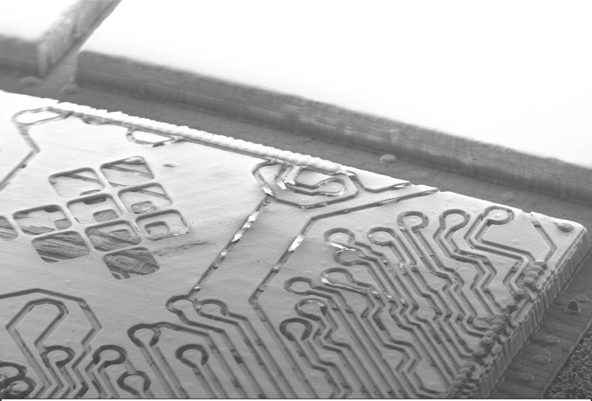
TESCAN ORSAY HOLDING, a.s. has described an A15 semiconductor failure analysis workflow that connects X-ray CT, ultrafast laser processing, optical and confocal microscopy, and SEM for progressive access to buried structures.
HORIBA Scientific announced the CiCi-Raman engine for high volume OEM industrial customers. The CiCi-Raman-785 features a deep-cooled Syncerity CCD camera with a new VIS-NIR detector and QE of 90% at 700nm.
This week in nanotech
$751.8M raised
6 funding rounds · 37 deals tracked
New products
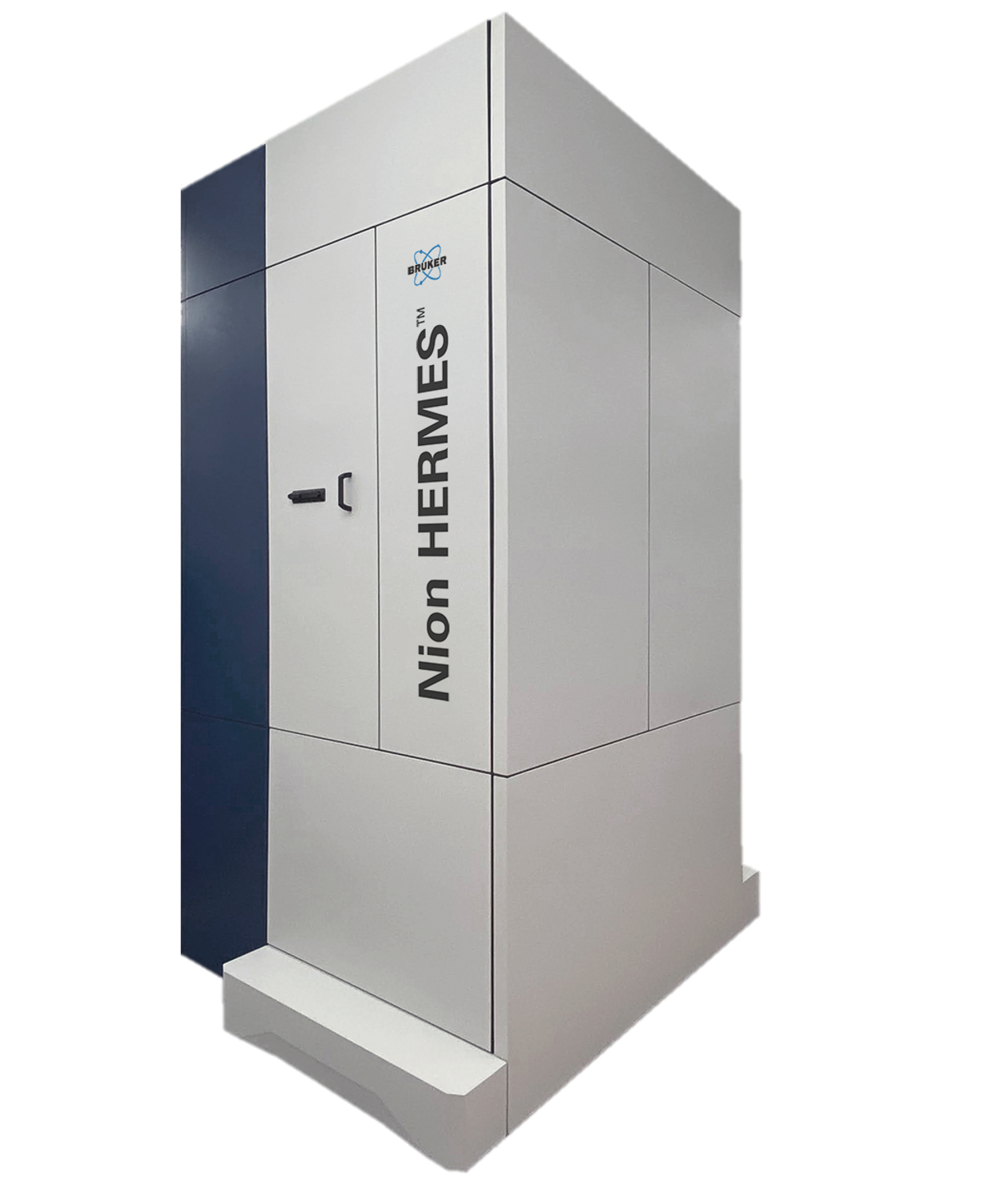 Nion-compatible In Situ STEM Holders for Electrical BiasingHummingbird Scientific Featured
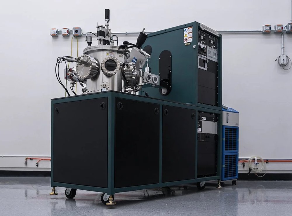 Orion Sputtering Deposition SystemsAJA International Featured
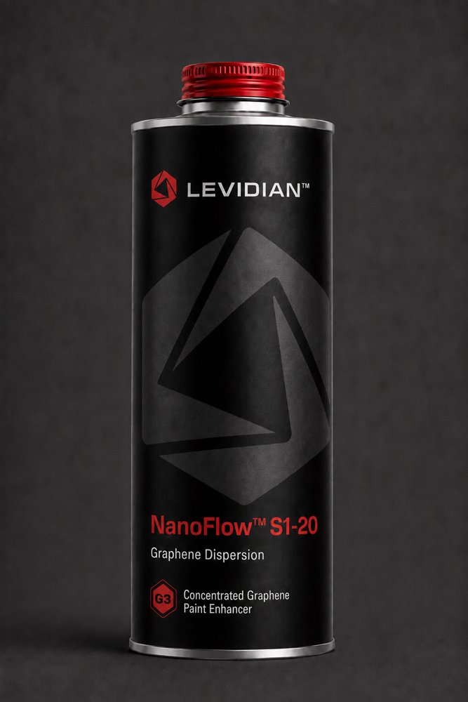 NanoFlow® S1-20Levidian
Market insights
Last 30 days: Quantum Technologies drew the most money: $3.18B.
Money raised per month